Provide One-stop Solutions For Si Materials
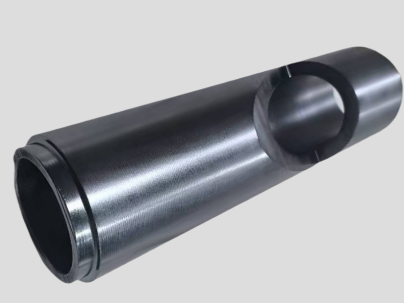
Monocrystalline and polycrystalline silicon profiled tubes by Jingge Semi are specialized components engineered for high-tech applications requiring exceptional material purity and structural precision. Leveraging ultra-high-purity silicon (99.9999%+), these tubes exhibit superior thermal stability, electrical insulation, and resistance to chemical corrosion. Their unique profiles can be custom-fabricated into complex shapes, such as tapered bends, multi-angle joints, or seamless liners for pipelines of varying diameters. A critical feature is their modular design, enabling precise splicing and alignment to fit intricate pipeline layouts, including tight corners , while maintaining vacuum integrity and minimal contamination risks. Widely used in semiconductor fabrication, photovoltaic systems, and ultra-clean fluid transfer, these silicon tubes ensure reliability in extreme environments.
Jingge Semi’s silicon seed crystal is a highly ordered, monocrystalline structure used to initiate the growth of large silicon ingots in processes like the Czochralski (CZ) method. As a critical component in semiconductor manufacturing and photovoltaic cell production, the seed crystal’s crystallographic orientation (e.g., <100> or <111>) directly determines the quality and efficiency of the final silicon wafer.
During crystal growth, the seed is dipped into molten silicon and slowly withdrawn, enabling atoms to align precisely with the seed’s lattice structure. This process ensures minimal defects and high purity, essential for applications in microelectronics and solar energy. Advanced techniques focus on optimizing seed crystal preparation, thermal stress management, and orientation control to meet the rising demand for high-performance silicon-based devices.
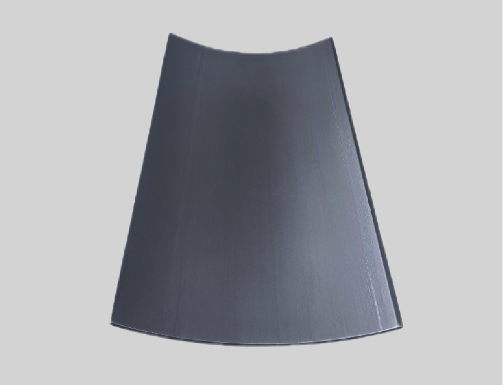
Tile-shaped curved silicon wafers by Jingge Semi are specialized substrates designed for non-traditional applications in semiconductor manufacturing, MEMS (Micro-Electro-Mechanical Systems), and advanced optical systems. Unlike standard planar wafers, these arc-shaped silicon components enable compact integration in space-constrained devices, such as biomedical sensors, microfluidic chips, and ultra-miniaturized actuators.
Through advanced lithography and anisotropic etching techniques, these wafers achieve complex geometries (e.g., curved edges, micro-cavities, or 3D patterns) while preserving crystalline integrity and electrical properties. This capability is critical for developing high-frequency RF devices, miniaturized inertial sensors, and optical waveguides.
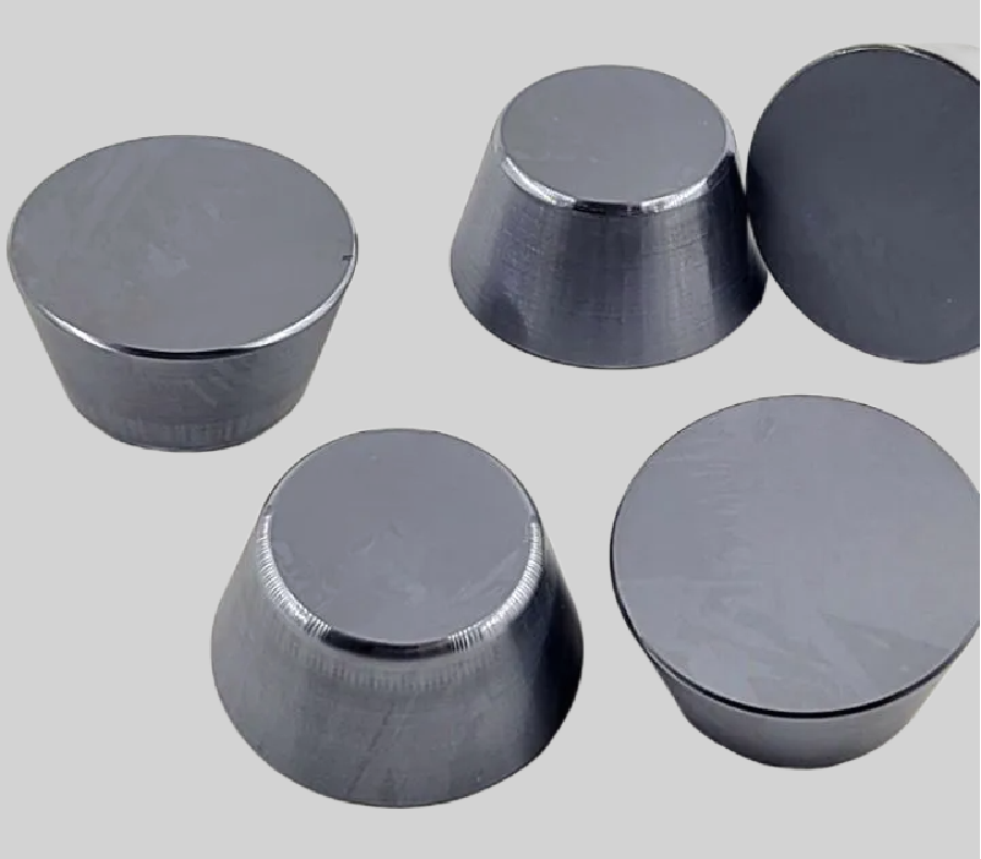
Jingge Semi’s silicon blocks are critical components in semiconductor, photovoltaic, and advanced electronics industries. Our precision custom silicon processing services utilize state-of-the-art CNC machining, diamond cutting, and chemical etching technologies to deliver micron-level accuracy. Specializing in semiconductor-grade (6N+ purity) and crucible-grown monocrystalline silicon, we provide tailored solutions for optical systems, quantum computing chambers, and MEMS device substrates. All blocks undergo rigorous crystalline structure verification and surface flatness testing (<0.5μm Ra). With ISO 9001-certified cleanroom facilities, we ensure contamination-free processing for applications requiring extreme thermal stability (up to 1400°C) and ultra-low defect densities (<0.1/cm²). Custom doping profiles and orientation markings available.
Perforated silicon wafers are ultra-thin substrates with precisely engineered micro-holes, widely used in semiconductor, MEMS, photonics, and biomedical industries. Customized drilling (via laser or plasma etching) enables micron-level accuracy, ensuring optimal performance in applications like optical filters, sensors, and microfluidic devices. These wafers are fabricated from high-purity monocrystalline silicon, offering exceptional thermal stability and electrical properties. Tailored to meet client specifications—including hole diameter, spacing, and pattern complexity—they support innovation in next-gen technologies. Trusted by OEMs for rapid prototyping and bulk production.Jingge Semi perforated wafers adhere to ISO-certified standards, delivering reliability for critical industrial and research needs.
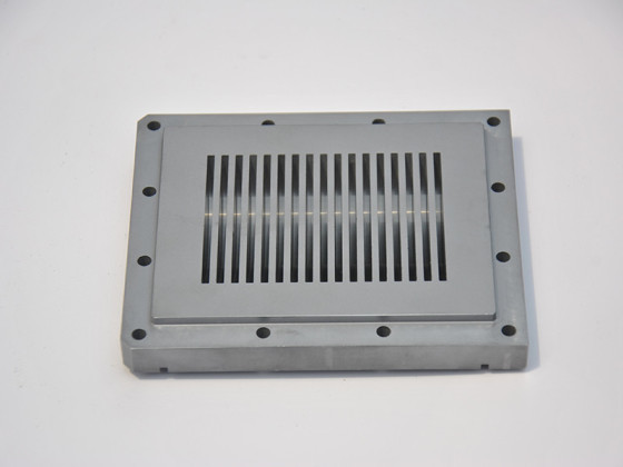
Jingge Semi’s CNC machining services specialize in crafting high-performance custom silicon parts for industries requiring extreme accuracy and material reliability. Utilizing advanced CNC technology, we deliver precision-machined silicon components with tight tolerances (±0.005mm), ideal for medical devices, electronics, automotive, and aerospace applications. From rapid silicon prototyping to low-volume production, we ensure superior surface finishes, chemical resistance, and thermal stability. Our expertise covers medical-grade silicon machining and complex geometries, supported by strict quality control (ISO-certified). Partner with us for fast turnaround, competitive pricing, and tailored solutions that meet your exact specifications.
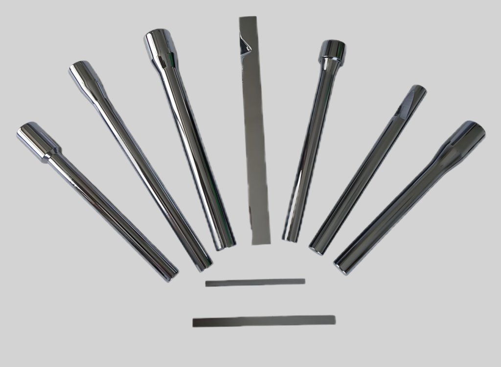
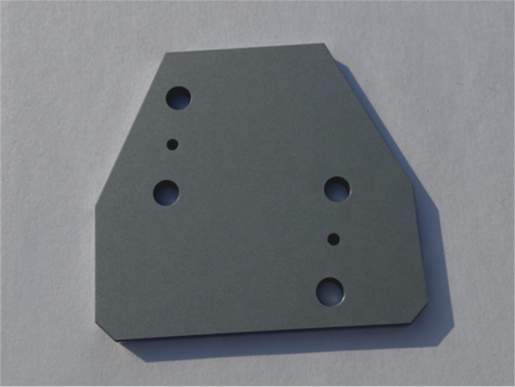
Jingge Semi specializing in custom silicon shaped parts and threaded components, our machining services focus on high-purity crystalline silicon for demanding applications in semiconductor, optics, and advanced industrial systems. Leveraging CNC machining, diamond cutting, and ultra-precision threading technologies, we deliver micron-level accuracy for complex geometries, internal/external threads, and intricate surface profiles. Our processes ensure exceptional dimensional stability, minimal micro-cracks, and sub-micron surface finishes, meeting stringent requirements for vacuum environments, chemical resistance, and high-temperature operations. From micro-threaded connectors to non-standard silicon fixtures, we tailor solutions to optimize performance in critical technical applications.
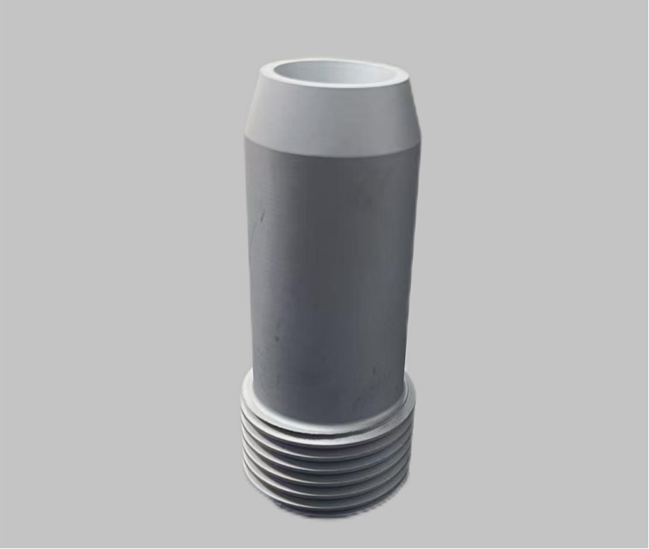
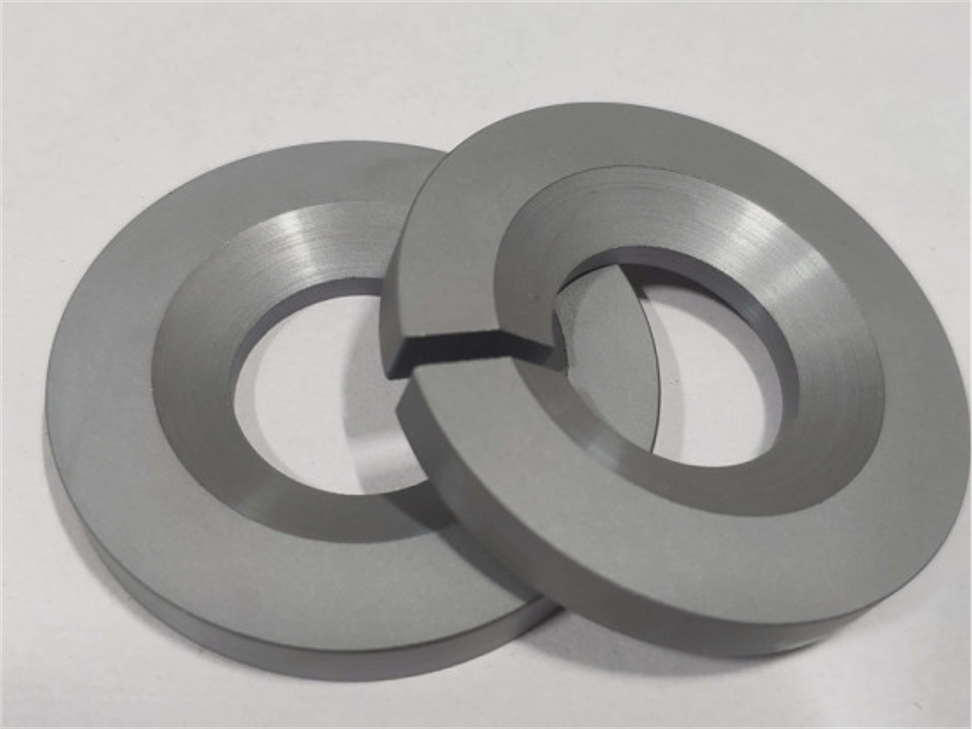
Threaded silicon tubes are precision-engineered components made from high-purity monocrystalline or polycrystalline silicon, widely used in semiconductor manufacturing, photovoltaic systems, and laboratory equipment. These tubes feature customizable threaded designs for secure connections in high-vacuum or high-temperature environments. During processing, advanced CNC machining enables variable diameter adjustments, ensuring compatibility with diverse industrial specifications. The material’s exceptional thermal stability, corrosion resistance, and electrical insulation make it ideal for critical applications. Customizable threading patterns and tapered profiles further enhance adaptability, meeting stringent requirements in aerospace, optics, and chemical processing industries.