Provide One-stop Solutions For Si Materials
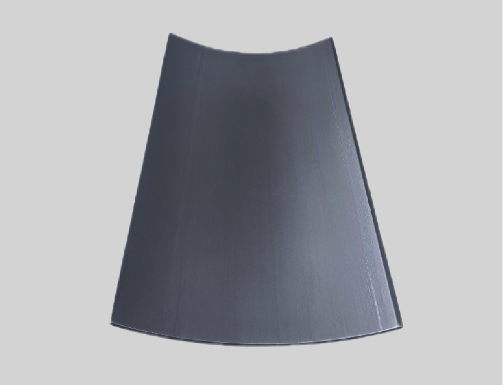
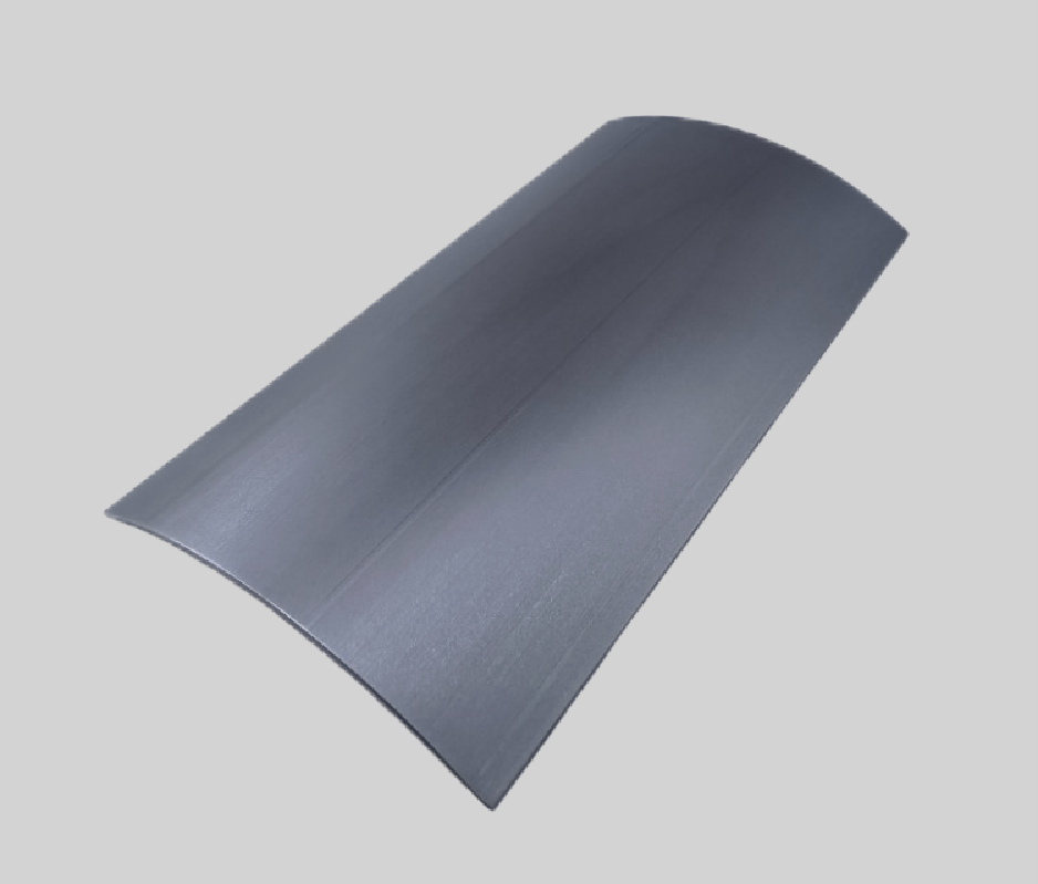
- Curvature Control: High-precision bending capabilities (e.g., 5–50 mm radii) for solar concentrators, automotive sensors, and curved displays.
- Material Versatility: Ultra-high-purity silicon (≥99.9999%) with doping options (p-type/n-type) to optimize conductivity for power devices or photovoltaics.
- Thickness Flexibility: Ranges from 10mm to 1000mm , supported by advanced thinning processes.
Technical Parameters
| No. | Characteristic | Unit | Spec |
|---|---|---|---|
| 1 | Purity | % | >6N/9N |
| 2 | Material | / | Mono / Poly |
| 3 | Diameter scale | mm | 0~600 / Customizable |
| 4 | Type/Contains | / | P type/ N type |
| 5 | Resistivity | Ω•cm3 | <0.02 / 1~4 / 60~90 |
| 6 | Crystal Orientation | / | (100)、(111)、(110) |
| 7 | Product Length | mm | 1~1000 |
| 8 | Surface treatment | / | Polishing |
Technical Advantages
Ultra-Precise 3D Geometry Control:Achieve complex shapes (arcs, micro-cavities, tile patterns) via advanced lithography and anisotropic etching, enabling seamless integration into compact, high-density microdevices.
Stress-Engineered Structural Integrity:Proprietary stress-relief technology minimizes mechanical deformation during shaping, ensuring stability for quantum computing modules and aerospace-grade sensors.
Enhanced Signal Performance in RF & Optical Systems:Curved surfaces reduce signal loss in high-frequency RF circuits and improve light coupling efficiency for optical waveguides and photonic chips.
Customizable Surface Microstructures:Tailor micro-grooves, nano-patterns, or textured edges to optimize functionality in MEMS actuators, lab-on-a-chip devices, and biomedical implants.
High Thermal and Chemical Resistance:Maintain performance under extreme environments (e.g., high-temperature semiconductor processes or corrosive medical diagnostics).