Provide One-stop Solutions For Si Materials
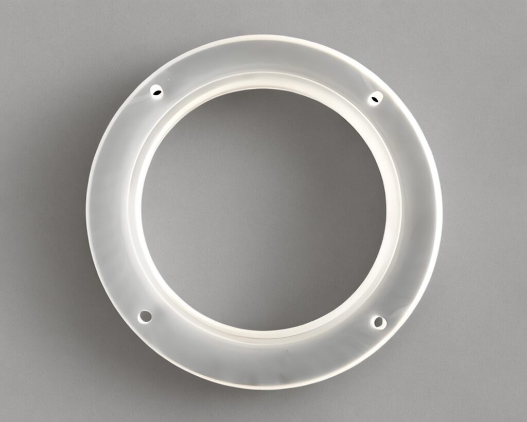
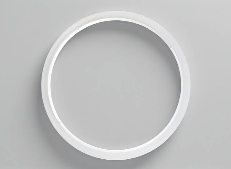
Home / Products / Quartz Part / Quartz Ring
- Ultra-low thermal expansion (≈0.55×10⁻⁶/°C), ensuring resistance to thermal shock.
- Chemical inertness (except for hydrofluoric acid and hot phosphoric acid), ideal for corrosive processes.
- High optical transmission (99.9% in UV to IR ranges), making them suitable for light-sensitive applications.
Technical Parameters
| No. | Characteristic | Spec |
|---|---|---|
| 1 | Density | 2.20g/cm3 |
| 2 | Mohs hardness | 5.5~6.5 |
| 3 | Tensile strength | 4.8x10^7 Pa (N/mm2) (7000 psi) |
| 4 | Compressive strength | >1.1x10^9 Pa (160,000 psi) |
| 5 | Bulk modulus | 3.7x10^10 Pa (5.3x10^6 psi) |
| 6 | Poisson's ratio | 0.17 |
| 7 | Thermal expansion | 5.5x10^-7cm/cm.°C (20°C-320°C) |
| 8 | Thermal conductivity | 1.4 W/m.°C |
| 9 | Softening point | 1683°C |
| 10 | Annealing point | 1215°C |
| 11 | Strain point | 1120°C |
Technical Advantages
Ultra-High Purity (99.99%+): Precision-engineered quartz rings ensure contamination-free performance in semiconductor etching and MEMS fabrication.
Superior Thermal Stability: Withstands extreme temperatures (up to 1,200°C) without deformation, critical for plasma etching and high-power laser systems.
Plasma-Optimized Surface: Advanced fractal modeling reduces ion scattering, enhancing etching uniformity and wafer yield by 15-20%.
Chemical Inertness: Resists corrosive gases (e.g., CF₄, Cl₂) and acids, extending service life in harsh semiconductor environments.
Low Thermal Expansion (5.5×10⁻⁷/°C): Maintains dimensional precision under rapid thermal cycling for consistent alignment in optical vacuum flanges.
MEMS-Ready Surface Finish: Sub-nanometer roughness (<0.5nm Ra) minimizes resonator damping, boosting MEMS gyroscope sensitivity.
Dual-Phase Sputtering Performance: Dense quartz structure enables high deposition rates (≥50 Å/s) with <0.1% particle generation for thin-film uniformity.
Plasma-Enhanced Durability: Chlorination-purified surfaces reduce particle shedding by 90% in 300mm wafer etchers.