Provide One-stop Solutions For Si Materials
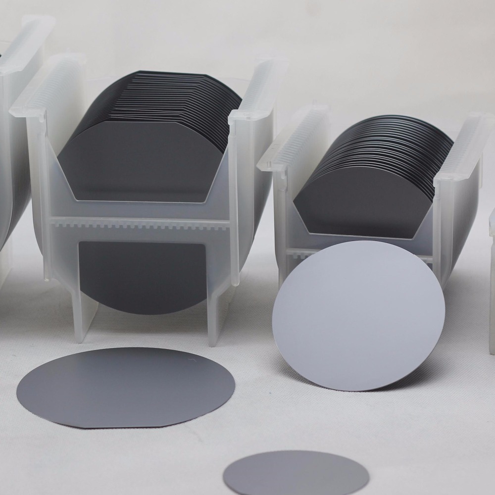
Covering diameters from 2-inch (50.8mm) to 6-inch (150mm), Jingge’s silicon wafers are engineered for versatility across semiconductor R&D, MEMS production, and industrial applications. Available in Prime (ultra-low defects, <0.5nm Ra), Test (equipment validation), Dummy (process calibration), and Reclaimed (cost-effective recycling) grades, these substrates support both double-side polished (DSP) and single-side polished (SSP) finishes. Prime-grade wafers achieve resistivity uniformity (±3%) with oxygen content <7ppma, ideal for advanced IC prototyping. All sizes feature thickness tolerance ±15μm, TTV <5μm, and particle control <20/cm², complying with SEMI standards. Customizable doping (Boron/Phosphorus), crystal orientations (100/110/111), and edge profiles ensure compatibility with 150mm-300mm fab ecosystems. Reclaimed wafers reduce costs by 50% while maintaining production-grade cleanliness for non-critical processes.

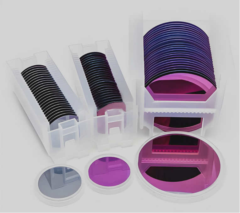
Jingge’s silicon oxide wafer (SiO2 wafer) is a critical material in semiconductor and microelectronics industries, formed by oxidizing a silicon substrate to create a thin, uniform layer of silicon dioxide. This oxide layer serves as an insulating barrier, passivation coating, or dielectric component in integrated circuits (ICs), MEMS devices, and photovoltaics. With excellent thermal stability, high dielectric strength, and compatibility with photolithography processes, SiO2 wafers are essential for manufacturing transistors, sensors, and optical components. Their thickness (ranging from nanometers to micrometers) and purity are tailored for applications in etching, masking, or gate oxide layers, making them indispensable in advanced electronics and nanotechnology.
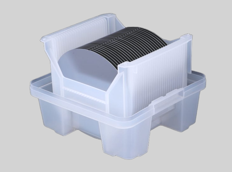
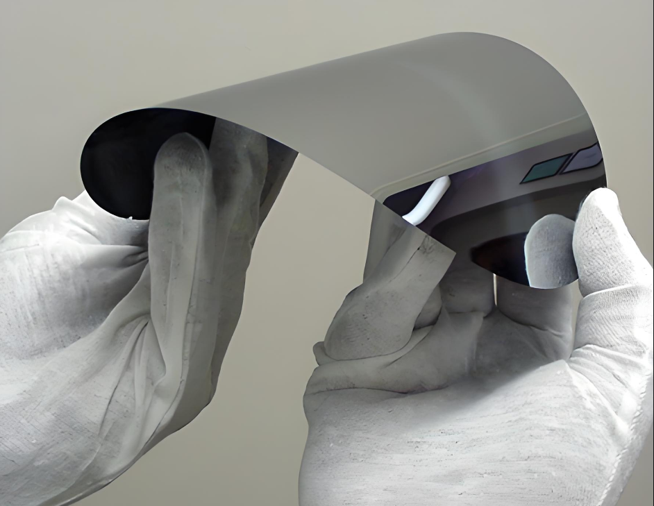
Silicon substrate is a high-purity crystalline silicon wafer widely used in semiconductor manufacturing, photovoltaic cells, and microelectromechanical systems (MEMS). It serves as the foundational layer for fabricating integrated circuits (ICs), solar panels, and sensors. Key properties include ultra-flat surfaces (≤1nm roughness), precise thickness (e.g., 200-775μm), and controlled doping (p-type/n-type) to enable electron mobility optimization. Advanced silicon substrates are produced through the Czochralski process, followed by slicing, polishing, and cleaning to meet ISO 5 cleanroom standards. With applications spanning 5G chips, AI processors, and renewable energy, silicon substrates remain critical to next-generation electronics and green technologies.
Custom silicon wafers are engineered to meet precise technical requirements for advanced semiconductor, photovoltaic, and MEMS applications. These wafers offer tailored resistivity levels (from low to high) to optimize electrical performance for specific devices. Thickness customization (ranging from ultra-thin 50μm to standard 750μm+) ensures compatibility with mechanical and thermal demands. Beyond traditional circular formats, manufacturers provide unique dimensional options, including rectangular silicon wafers for space-efficient designs and ultra-large diameter wafers (up to 450mm) to enhance production scalability. Surface finishes, crystal orientations, and edge profiles can also be adjusted, making custom wafers ideal for specialized sensors, power electronics, and cutting-edge optoelectronics systems.
Quartz Wafers are ultra-pure, high-stability substrates widely used in advanced industries such as semiconductor manufacturing, photolithography, and optical device production. Made from high-purity quartz (SiO₂), these wafers exhibit exceptional thermal stability, chemical resistance, and low thermal expansion, making them ideal for applications like photolithography masks, MEMS sensors, and laser optics. Precision-polished to achieve nanometer-level flatness, quartz wafers ensure reliability in extreme environments, including high-temperature semiconductor processes. Their role in enabling cutting-edge technologies, from 5G communications to quantum computing, underscores their critical importance in modern electronics and photonics industries.