Provide One-stop Solutions For Si Materials
- Material Advantages:Monocrystalline Silicon exhibits uniform lattice structure, ideal for semiconductor-grade applications.Polycrystalline Silicon cost-effective with excellent thermal conductivity, widely used in solar energy and industrial pipelines.
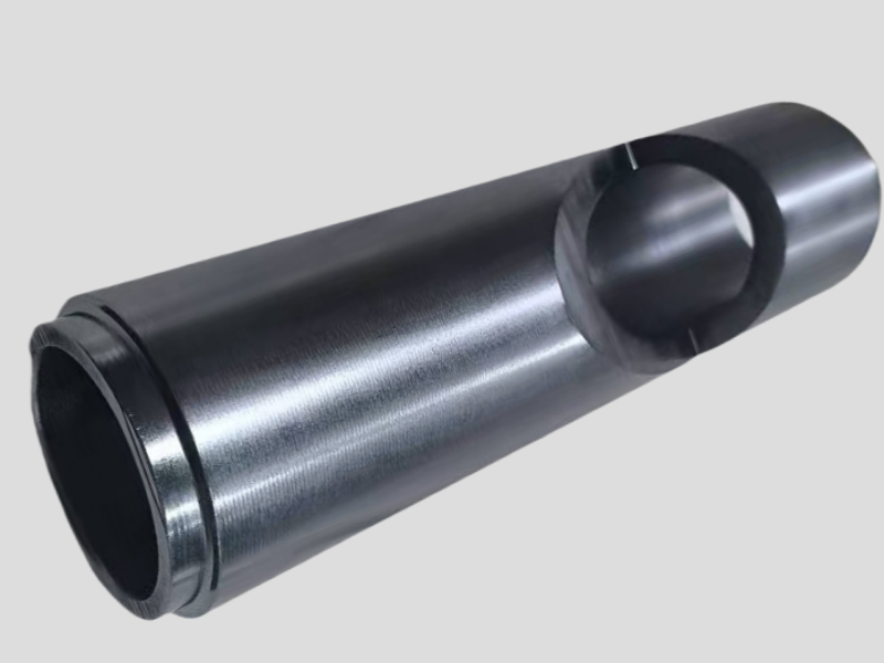
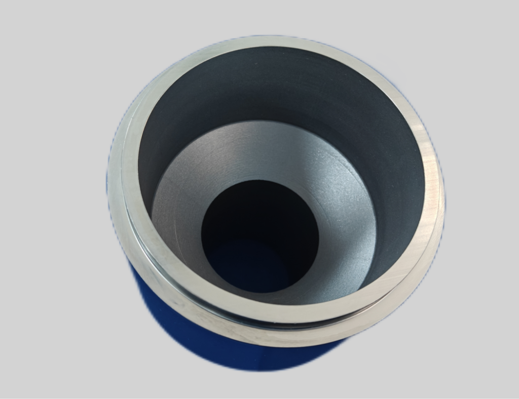
- Customization:Available in diameters from 1 mm to 1000 mm, with tolerance control down to micrometers.Surface treatments (e.g., polished, etched) enhance corrosion resistance and flow efficiency.
- Interlocking Design:Patented connectors simplify assembly at pipe junctions, reducing installation time by 30%.
Technical Parameters
| No. | Characteristic | Unit | Spec |
|---|---|---|---|
| 1 | Purity | % | >6N/9N |
| 2 | Material | / | Mono / Poly |
| 3 | Diameter scale | mm | 0~1300 / Customizable |
| 4 | Type/Contains | / | P type/ N type |
| 5 | Resistivity | Ω•cm3 | <0.02 / 1~4 / 60~90 |
| 6 | Crystal Orientation | / | (100)、(111)、(110) |
| 7 | Operating Temperature | ℃ | <1250 ℃ |
| 8 | Surface treatment | / | Polishing |
Technical Advantages
Cost-Effective High-Temperature Solution:Ideal for oxidation/annealing processes below 1000°C, offering 40% cost savings versus monocrystalline alternatives.
Enhanced Thermal Shock Resistance:Grain boundary structure absorbs thermal stress, reducing crack risks in rapid thermal cycling applications.
Compatibility with Legacy Processes:Proven reliability in 150mm/200mm wafer manufacturing for power devices and analog ICs, with minimal process re-qualification.
Batch Process Scalability:Supports large-volume production with cycle lifetimes exceeding 5,000 runs in non-critical contamination environments.
Customizable Surface Texturing:Engineered contact points minimize wafer imprinting while maintaining alignment stability for 8-inch wafer batches.