Provide One-stop Solutions For Si Materials
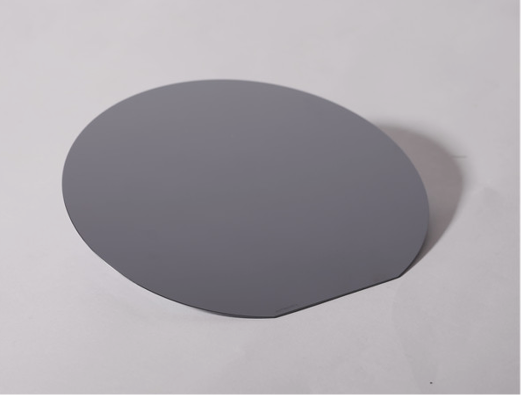
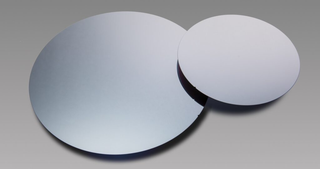
Jingge’s silicon substrate is a ultra-pure, monocrystalline silicon wafer engineered to serve as the base material for advanced semiconductor devices. Key characteristics include high resistivity (1-10,000 Ω·cm), low defect density (<1 defect/cm²), and excellent thermal stability (up to 1,200°C). A prominent variant is the Silicon-on-Insulator (SOI) substrate, which features a layered structure of silicon-insulator-silicon. This design minimizes parasitic capacitance and leakage currents, making SOI ideal for high-frequency RF chips, energy-efficient power devices, and radiation-hardened aerospace electronics.
Photovoltaics: Thinned substrates (150-200μm) with anti-reflective coatings for solar cells.
MEMS: Double-side polished wafers with sub-nanometer surface roughness.
5G/IoT: SOI substrates enable low-loss millimeter-wave communication.
Automotive: High-power SiC (Silicon Carbide) epitaxial substrates for EV inverters.
Technical Parameters
| Project | Content |
|---|---|
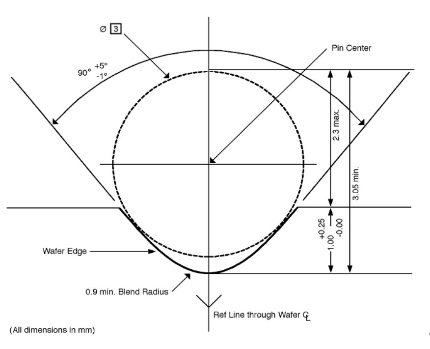
| Diameter | 2"(50.8mm)、3"(76.2mm)、4"(100mm)、5"(125mm)、6"(150mm)、8"(200mm)、12"(300mm) |
| Grade | Prime、Test、Dummy、Reclaimed |
| Growth Method | CZ、FZ |
| Orientation | 100 , 111 , 110 |
| Type/Dopant | P Type/Boron、 N Type/Phos、 N Type/As、N Type/Sb |
| Resistivity | From 0.001 to 10000 ohm-cm |
| Thickness (μm) | 50~3000μm |
| Thickness Tolerance | Standard ± 25μm、Maximum Capabilities ± 5μm |
| TTV (μm) | Standard < 10 um、Maximum Capabilities <5 um |
| Bow/Warp (μm) | Standard <40 um、Maximum Capabilities <20 um |
| Finish | As cut、Lapped、 Etched、 SSP、DSP、etc |
| Off cut | up to 7 deg |
| Particle | <10@0.5um、<10@0.3um、 <10@0.2um |
Technical Advantages
Zero Defect Monocrystalline Structure:Engineered with <0.3 defects/cm² via AI-driven Czochralski growth, maximizing chip yield for 3nm/2nm advanced nodes in AI and HPC applications.
SOI Substrate Power Efficiency:Reduce energy loss by 40% with our Silicon-on-Insulator (SOI) technology, featuring a buried oxide layer (BOX ≤25nm) for ultra-low leakage in 5G RF front-ends and IoT edge devices.
Atomic-Level Surface Perfection:Achieve Ra ≤0.15nm surface roughness through proprietary CMP technology, enabling defect-free EUV lithography and quantum dot laser fabrication.”
Extreme Thermal & Mechanical Stability:Operate flawlessly in -60°C to 1,300°C environments, validated for SiC/GaN epitaxy in EV traction inverters and satellite power systems.”
Application-Specific Customization:From ultra-thin 100μm SOI wafers (photonics) to 800μm heavy-doped substrates (IGBT modules), we deliver ±0.5% thickness uniformity and doping precision.