Provide One-stop Solutions For Si Materials
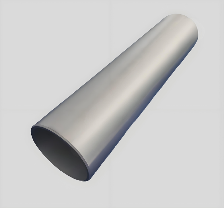
- Monocrystalline Silicon Tube Targets
- Manufacturing: Produced via the Czochralski (CZ) method, a melt-growth technique that ensures defect-free, uniform crystal structures.
- Purity: Exceeds 99.9999% (semiconductor grade), with controlled resistivity (0.005–0.020 Ω·cm) for optimal electrical conductivity.
- Applications: Ideal for advanced semiconductor devices (e.g., 5nm/3nm logic chips, DRAM) and high-frequency electronics due to their superior charge carrier mobility.
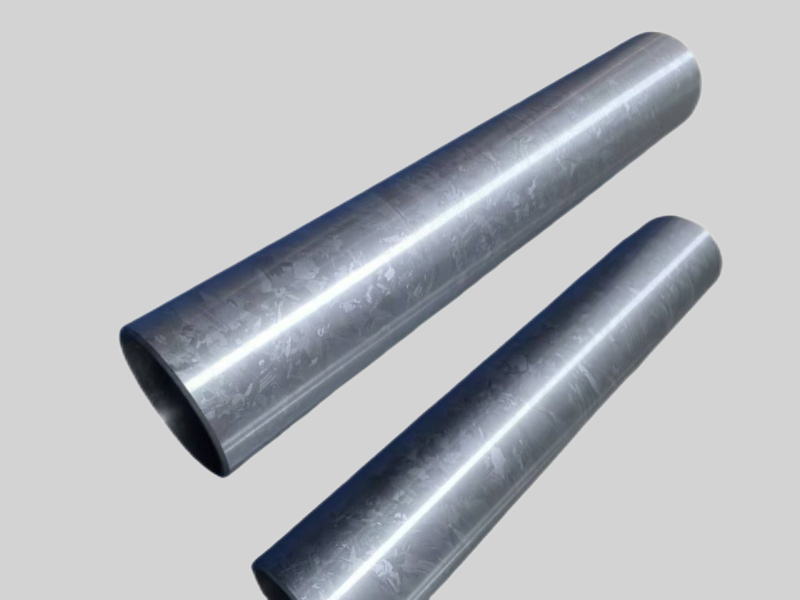
- Polycrystalline Silicon Tube Targets
- Manufacturing: Prepared using the Siemens process or upgraded metallurgical refining, balancing cost efficiency and scalability .
- Purity: Solar-grade purity (99.999%) supports high-efficiency solar cells (e.g., PERC, TOPCon) and thin-film transistors (TFTs) .
- Advantages: Cost-effective for large-scale PV production while maintaining excellent light absorption and thermal stability.
Technical Parameters
| No. | Characteristic | Unit | Spec |
|---|---|---|---|
| 1 | Purity | % | >6N |
| 2 | Material | / | Mono / Poly |
| 3 | Diameter scale | mm | 0~2000 / Customizable |
| 4 | Type/Contains | / | P type/ N type |
| 5 | Resistivity | Ω•cm3 | <0.02 / 1~4 / 60~90 |
| 6 | Crystal Orientation | / | (100)、(111)、(110) |
| 7 | Dopant | / | B、P、Ga、As、Sb |
| 8 | Ra | um | ≤0.8 |
Technical Advantages
Seamless One-Piece Design Up to 1500mm:Achieve uninterrupted thin-film deposition withmonolithic silicon tube targets, eliminating joint defects for quantum devices and high-precision optics.
Wide Diameter Customization (10mm–600mm):Adapt to any PVD system configuration, from micro-scale MEMS sensors to industrial solar cell coating, with precision-engineered cylindrical targets.
Ultra-High Purity (99.9999%) Monocrystalline Tubes:Ensure defect-free semiconductor films for advanced ICs and photonic applications, certified for ISO Class 3 cleanroom processes.
Cost-Efficient Polycrystalline Solutions:Reduce material waste by 30% using segmented polycrystalline silicon tubes, ideal for large-area wear-resistant coatings.
Enhanced Coating Uniformity in Rotational Sputtering:Optimize thin-film homogeneity with cylindrical geometry, achieving <1% thickness variation in 3D component coatings.
Dual Resistivity Control (0.001Ω·cm to 100Ω·cm):Tailor electrical properties for RF components, power devices, or insulating layers with customized doping profiles.
Rapid Thermal Conductivity & Stability:Minimize thermal stress in high-power sputtering with crystalline silicon’s superior heat dissipation, extending target lifespan by 40%.