Provide One-stop Solutions For Si Materials
- ESD Protection: Anti-static variants (e.g., carbon-filled polypropylene) ensure electrostatic discharge (ESD) safety, with surface resistivity levels compliant with ANSI/ESD S20.20 standards.
- High-Temperature Resistance: Si carriers withstand extreme temperatures up to 1200°C, making them ideal for high-temperature applications like annealing.
- Chemical Compatibility: Resistant to aggressive chemicals used in semiconductor processing, such as hydrofluoric acid.
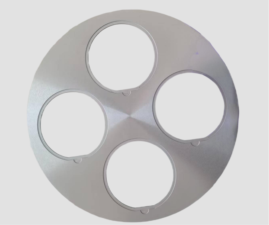
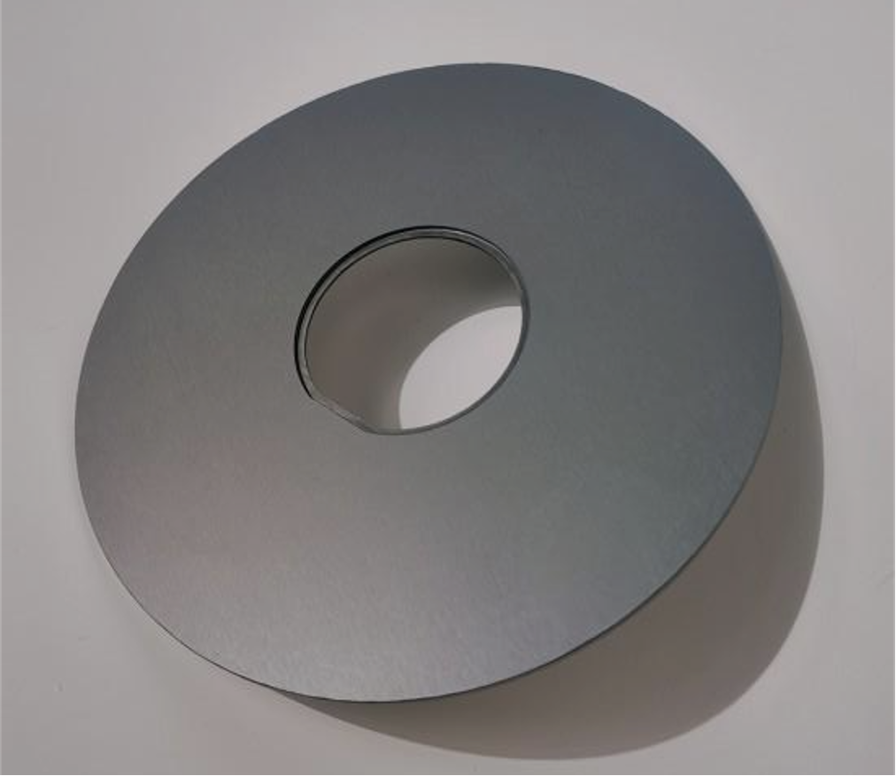
- Customization: Available in sizes from 1″ to 150mm (25–300mm) with vacuum pockets,and flat/notch alignments.
Technical Parameters
| No. | Characteristic | Unit | Spec |
|---|---|---|---|
| 1 | Purity | % | >6N |
| 2 | Material | / | Mono / Poly |
| 3 | Diameter scale | mm | 0~800 / Customizable |
| 4 | Type/Contains | / | P type/ N type |
| 5 | Resistivity | Ω•cm3 | <0.02 / 1~4 / 60~90 |
| 6 | Crystal Orientation | / | (100)、(111)、(110) |
| 7 | Dopant | / | B、P、Ga、As、Sb |
| 8 | Surface treatment | / | Polishing |
Technical Advantages
Ultra-High Purity Material (99.99999%):Engineered with contamination-free silicon to prevent wafer surface defects in sensitive processes like EUV lithography and atomic layer deposition (ALD).
Plasma & Chemical Resistance:Withstands aggressive environments (e.g., Cl₂, O₂ plasma) and acidic/alkaline cleaning agents, ensuring long-term durability over 10,000+ process cycles.
Precision Wafer Alignment Technology:Laser-etched micro-grooves ensure sub-10μm positional accuracy, critical for high-throughput automated handling systems.
Thermal Shock Resilience:Stable performance across extreme temperatures (-196°C to 800°C), ideal for rapid thermal processing (RTP) and cryogenic applications.
Low Particle Generation (<0.1 particles/cm²):Mirror-polished surfaces (Ra <0.5nm) minimize micro-abrasion and contamination, boosting wafer yield to >99.95%.
Lightweight & High-Strength Design:Monocrystalline silicon structure reduces tool-induced wafer stress while maintaining 3x higher rigidity than quartz alternatives.