Provide One-stop Solutions For Si Materials
Quartz wafers are categorized into two primary types: single-crystal quartz (synthetic quartz crystal) and fused quartz (amorphous silica). Single-crystal quartz wafers, grown through advanced hydrothermal synthesis, offer exceptional crystalline uniformity and anisotropic properties, making them ideal for high-frequency SAW/BAW filters, piezoelectric sensors, and quantum computing components.
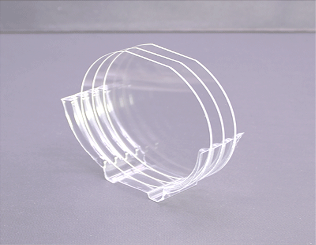
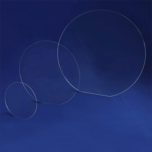
In contrast, fused quartz wafers are manufactured by melting ultra-pure silica into a non-crystalline form, renowned for isotropic thermal stability, near-zero thermal expansion, and UV transparency. These wafers dominate applications like photolithography masks, deep-UV laser optics, and semiconductor process chambers, where extreme heat resistance and optical precision are critical.
Technical Parameters
| Diameter | 2″ | 3″ | 4″ | 5″ | 6″ | 8″ |
| Thickness (um) | Depends on Request | |||||
| Material | Fused Silica | |||||
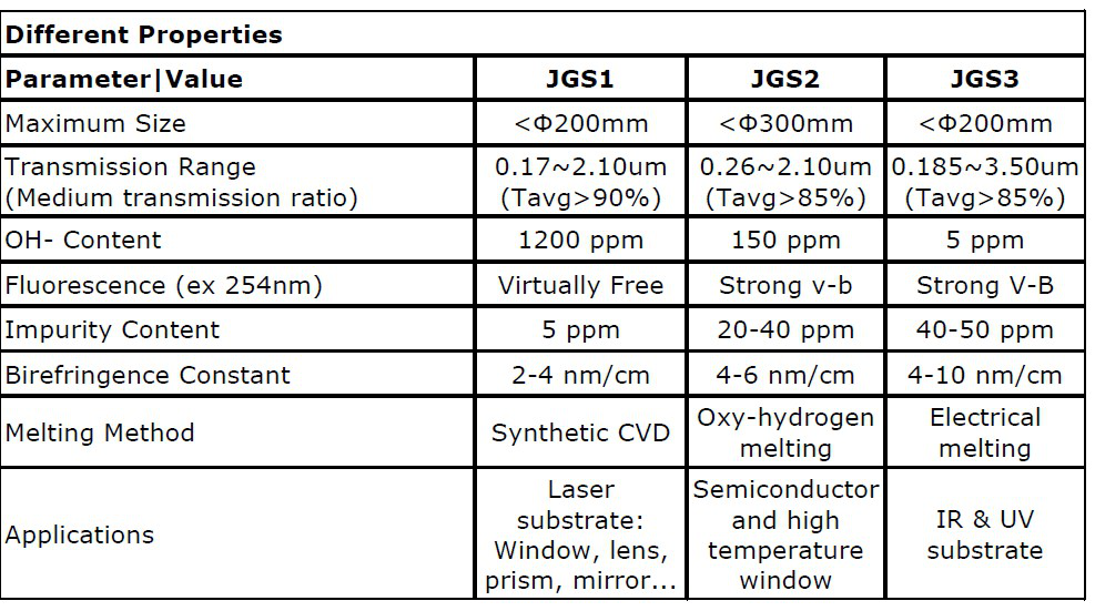
| Grade/Brand | JGS2/JGS1/JGS3 | |||||
| Surface Finished | DSP/SSP | |||||
| TTV (um) | <8 | <10 | <10 | <10 | <15 | <20 |
| Bow/Warp (um) | <30 | <30 | <40 | <40 | <60 | <60 |
| Ra (nm) | <1 | |||||
| S/D (um) | 40/20 | |||||
| Mechanical | Units of Measure | SI/Metric | (Imperial) |
| Density | gm/cc (lb/ft3) | 2.2 | -137.4 |
| Porosity | % (%) | 0 | 0 |
| Color | — | clear | — |
| Flexural Strength | MPa (lb/in2x103) | — | — |
| Elastic Modulus | GPa (lb/in2x106) | 73 | -10.6 |
| Shear Modulus | GPa (lb/in2x106) | 31 | -4.5 |
| Bulk Modulus | GPa (lb/in2x106) | 41 | -6 |
| Poisson’s Ratio | — | 0.17 | -0.17 |
| Compressive Strength | MPa (lb/in2x103) | 1108 | -160.7 |
| Hardness | Kg/mm2 | 600 | — |
| Fracture Toughness KIC | MPa•m1/2 | — | — |
| Maximum Use Temperature (no load) | °C (°F) | 1100 | -2000 |
| Thermal | |||
| Thermal Conductivity | W/m•°K (BTU•in/ft2•hr•°F) | 1.38 | -9.6 |
| Coefficient of Thermal Expansion | 10–6/°C (10–6/°F) | 0.55 | -0.31 |
| Specific Heat | J/Kg•°K (Btu/lb•°F) | 740 | -0.18 |
| Electrical | |||
| Dielectric Strength | ac-kv/mm (volts/mil) | 30 | -750 |
| Dielectric Constant | @ 1 MHz | 3.82 | -3.82 |
| Dissipation Factor | @ 1 MHz | 0.00002 | -0.00002 |
| Loss Tangent | @ 1 MHz | — | — |
| Volume Resistivity | ohm•cm | >1010 | — |
Technical Advantages
Superior Thermal Stability:Engineered with ultra-low thermal expansion (<5×10⁻⁷/°C), our quartz wafers maintain dimensional integrity even in extreme temperature cycles (up to 1200°C), ensuring reliability in high-power semiconductor processes and space-grade electronics.
Nanometer-Level Precision:Advanced polishing technology achieves sub-nanometer surface roughness (Ra ≤0.5nm), critical for EUV photolithography masks and MEMS sensor fabrication, minimizing signal loss and enhancing device yield.
Optical & UV Transparency:With >90% transmittance in deep-UV spectrum (190-250nm), fused quartz wafers enable cutting-edge excimer laser optics and DUV lithography systems, accelerating breakthroughs in chip miniaturization.
Piezoelectric Excellence:Single-crystal quartz wafers deliver unmatched frequency stability (Q-factor >10⁶), powering 5G/6G SAW filters and ultra-precise atomic force microscopy (AFM) probes.
Chemically Inert & Contamination-Free:High-purity SiO₂ (99.9999%) ensures zero outgassing and resistance to acids/plasma, ideal for semiconductor etching chambers and biomedical MEMS devices.
Customized Scalability:From 100mm to 450mm wafer diameters, our flexible manufacturing supports quantum computing substrates to aerospace sensor arrays, backed by ISO-certified cleanroom production.