Provide One-stop Solutions For Si Materials
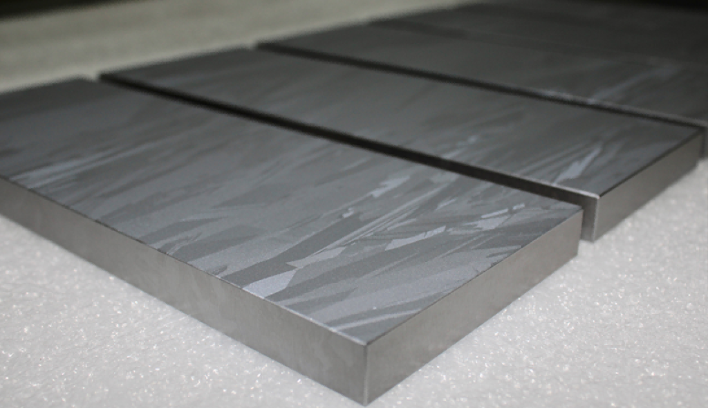
A silicon planar square target is a high-purity, rectangular-shaped material designed for advanced thin film deposition in industries such as semiconductor manufacturing and display panel production. Its square geometry maximizes material utilization and ensures uniform coating on large substrates, critical for lithography and TFT (Thin-Film Transistor) applications. With ultra-low oxygen content (<10ppm) and a defect-free surface, it guarantees stable sputtering performance in PVD processes, enabling high-quality conductive or insulating layers in microchips and OLED screens. Customizable in size and purity (up to 99.9999%), these targets meet the stringent requirements of modern precision electronics and optoelectronic devices.
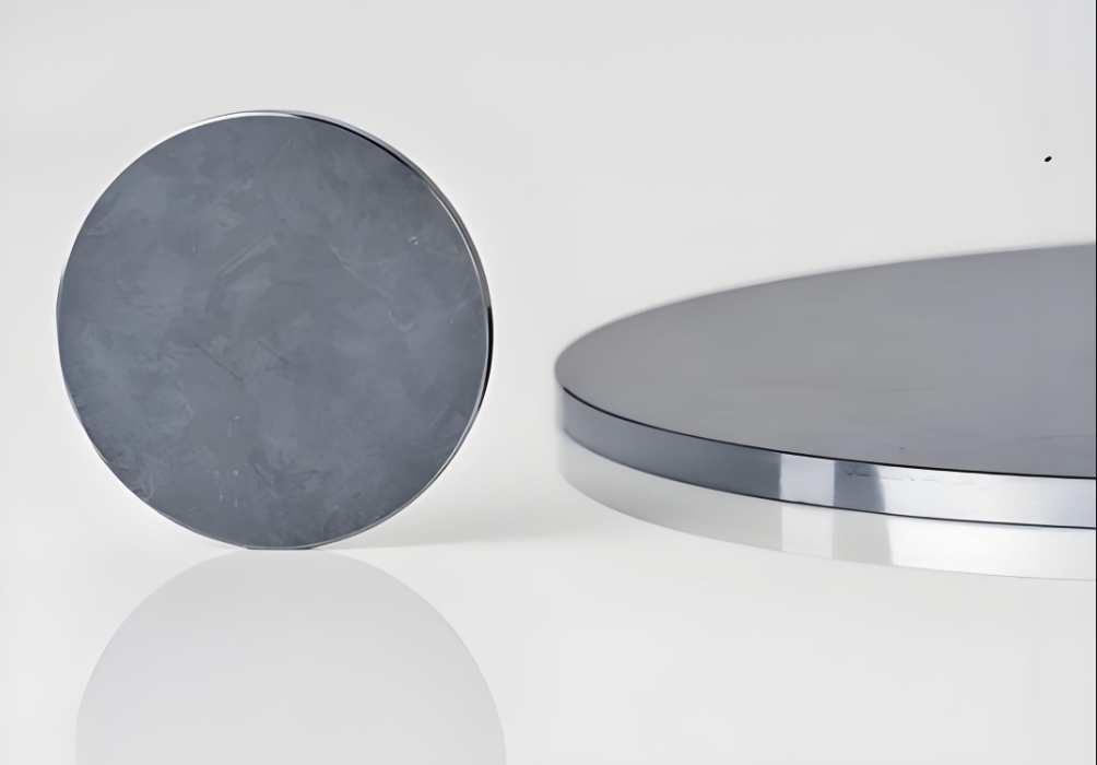
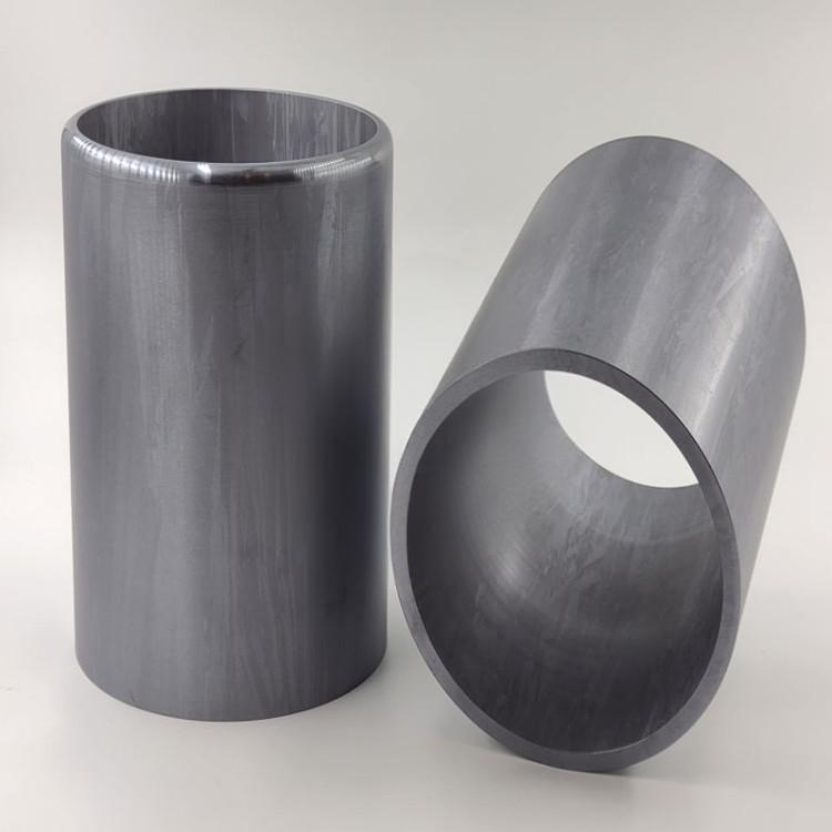
A silicon tubular target, engineered with a cylindrical rotating design, is a high-purity material optimized for large-area thin film deposition in industries such as photovoltaic cell production and semiconductor packaging. Its rotatable structure ensures uniform erosion and enhanced heat dissipation during sputtering (PVD), achieving material utilization rates exceeding 80%—significantly higher than traditional planar targets. With ultra-low impurity levels (99.9999% purity) and precise dimensional control, it enables consistent coatings on curved surfaces or complex 3D components. Customizable in diameter and length, these targets are vital for continuous manufacturing processes in solar panel assembly and advanced optical device fabrication.
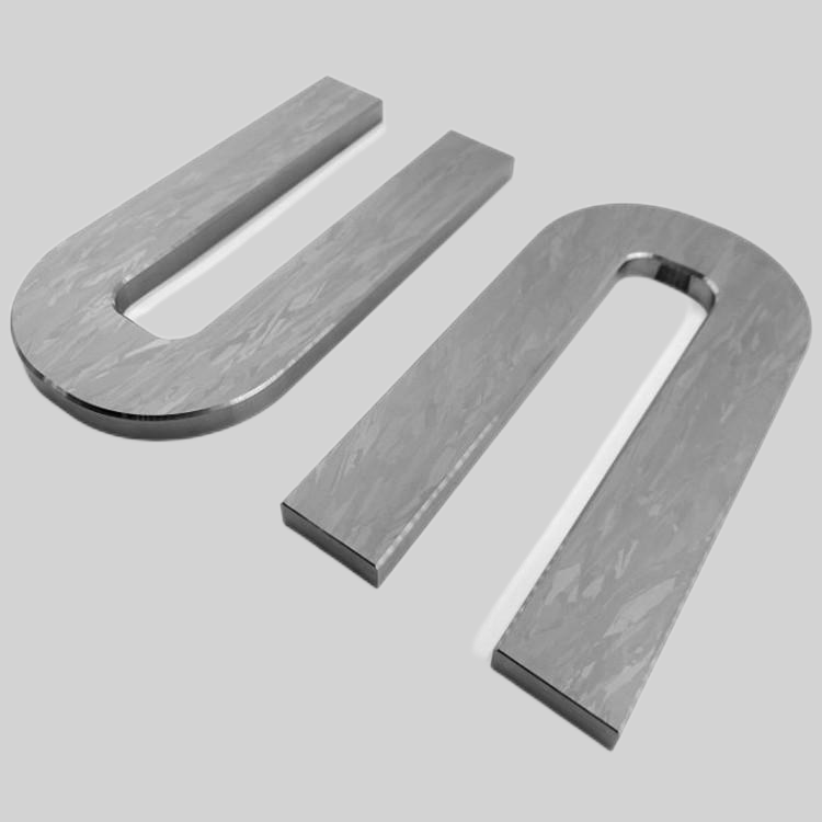
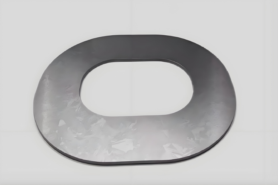
A custom-shaped silicon target is a high-purity, geometrically complex sputtering material designed for specialized thin film deposition in cutting-edge industries like MEMS, 3D chip packaging, and advanced sensor production. Its non-planar structure (e.g., curved, multi-angle, or micro-patterned) enables uniform coating on irregular substrates, critical for manufacturing miniaturized electronic components and optical microstructures. With ultra-low impurity levels (up to 99.99999% purity) and advanced CNC machining precision, these targets achieve optimal plasma distribution in multi-axis PVD systems while reducing material waste by 30-50% compared to standard targets. Customizable designs support unique industrial requirements, driving innovation in nanotechnology and quantum device fabrication.
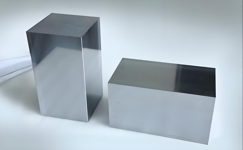
Silicon block and rod targets are high-purity solid-state materials designed for specialized thin film deposition in semiconductor and solar industries. The block form (rectangular/cubic) enables large-area uniform coating in CVD processes, while cylindrical rods excel in high-power rotating sputtering systems due to their axial symmetry and thermal stability. With purity levels up to 99.9999% and controlled crystal orientation, these targets minimize micro-cracks and particle generation during high-temperature operations. Customizable in dimensions (e.g., 200mm diameter rods or 300×300mm blocks), they are critical for manufacturing advanced logic chips, photovoltaic modules, and MEMS devices requiring ultra-clean interfaces.