Provide One-stop Solutions For Si Materials
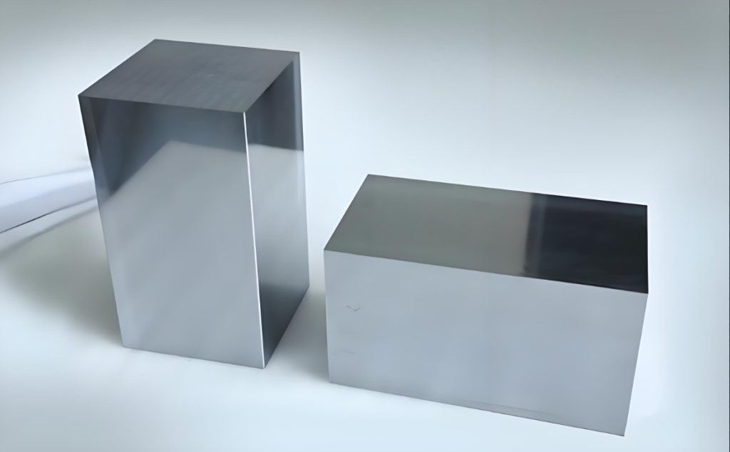
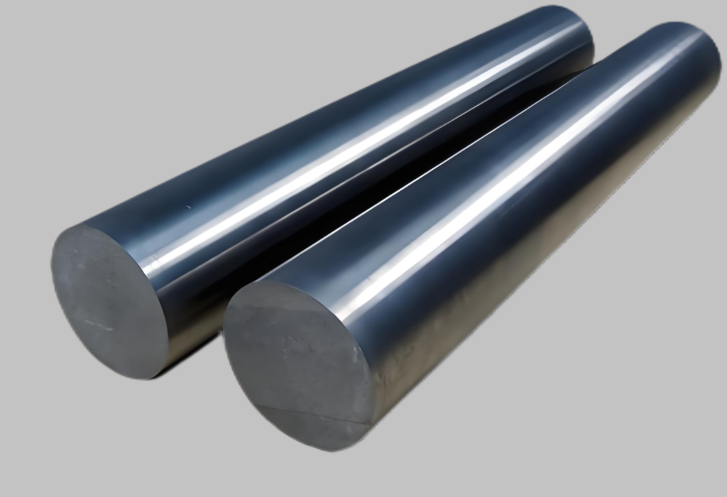
Silicon Ingots & Blocks are fundamental materials for semiconductor manufacturing, photovoltaic cells, and precision optics. Monocrystalline Silicon Blocks are characterized by ultra-high purity (99.9999%) and a uniform crystal structure, ideal for high-performance ICs and quantum computing components. Polycrystalline Silicon Rods provide cost-effective solutions for solar cell production and industrial coatings. Both types can undergo precision surface grinding and mirror polishing, achieving sub-nanometer roughness (Ra <0.5nm) to minimize defects in thin-film deposition. Available in standardized or custom geometries, these materials support advanced processes such as epitaxial growth, MEMS fabrication, and infrared optics, ensuring reliability in extreme thermal and electrical environments.
Technical Parameters
| No. | Characteristic | Unit | Spec |
|---|---|---|---|
| 1 | Purity | % | >6N |
| 2 | Material | / | Mono / Poly |
| 3 | Diameter scale | mm | 0~2000 / Customizable |
| 4 | Type/Contains | / | P type/ N type |
| 5 | Resistivity | Ω•cm3 | <0.02 / 1~4 / 60~90 |
| 6 | Crystal Orientation | / | (100)、(111)、(110) |
| 7 | Dopant | / | B、P、Ga、As、Sb |
| 8 | Ra | um | ≤0.8 |
Technical Advantages
Ultra-High Purity (99.9999%) Monocrystalline Blocks:Enable defect-free epitaxial growth for quantum devices and 5G RF chips, certified for ISO Class 2 cleanroom processes.
Sub-Nanometer Surface Finish (Ra <0.5nm):Achieve mirror-polished silicon blocks with laser-grade flatness, critical for EUV lithography and infrared optical substrates.
Polycrystalline Cost Efficiency & Scalability:Optimize solar cell production with low-cost polycrystalline silicon rods, reducing wafer processing costs by 20%.
Thermal Stability in Extreme Environments:Withstand temperatures up to 1300°C without structural degradation, ideal for high-power semiconductor devices and aerospace components.
Custom Geometry & Dimensional Precision:Supply silicon ingots in standard (100mm-450mm) or bespoke sizes, tailored for MEMS sensors, photonic circuits, and hybrid IC packaging.
Rapid Grinding-to-Polishing Turnkey Solutions:Deliver ready-to-use silicon blocks with <1μm dimensional tolerance within 3 weeks, accelerating R&D cycles for advanced optoelectronics.
Low Oxygen/Carbon Content (<1ppm):Minimize impurity-induced failures in high-voltage power devices and neutron detection systems.
Multi-Industry Compatibility:From semiconductor fabs to space-grade optics, our silicon ingots supportCzochralski (CZ), float-zone (FZ), and chemical etching processes.