
실리콘 소재를 위한 원스톱 솔루션 제공
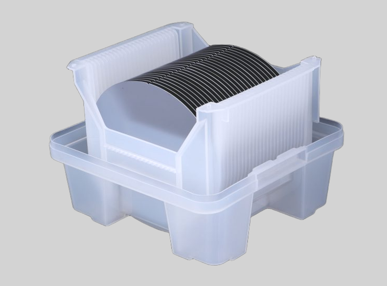
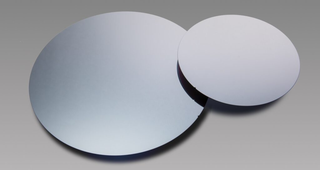
Jingge’s 200mm (8-inch) to 300mm (12-inch) silicon wafers are engineered for high-volume manufacturing of advanced logic ICs, 3D NAND, and CIS image sensors. Available in Prime (sub-0.2nm Ra surface, ≤0.3ppb metal contamination), Test (equipment stress testing), Dummy (thermal budget validation), and Reclaimed (post-process recycling) grades, these substrates support double-side polishing (DSP) for EUV lithography and single-side polishing (SSP) for epitaxial deposition.
Prime-grade 300mm wafers achieve total thickness variation (TTV) <1μm with ultra-low COP defects (<5/cm²), critical for sub-7nm node production. All wafers comply with SEMI M1/M73 standards, offering customizable parameters:
Resistivity: 0.001-10000 Ω·cm (p-type Boron/n-type Phosphorus)
Oxygen content: <12ppma (CZ/FZ crystal growth)
Edge exclusion: ≤2mm (300mm) / ≤1.5mm (200mm)
Reclaimed wafers reduce fab OPEX by 45% while maintaining ≤25 particles/addon (>0.2μm) for non-critical layers. Compatible with 450mm-ready automation systems, our 200-300mm portfolio enables seamless scaling from legacy 90nm to cutting-edge 3nm GAA architectures.
기술 사양
| 프로젝트 | 내용 |
|---|---|
| 직경 | 2"(50.8mm), 3"(76.2mm), 4"(100mm), 5"(125mm), 6"(150mm), 8"(200mm), 12"(300mm) |
| 등급 | Prime, Test, Dummy, Reclaimed |
| 성장 방법 | CZ, FZ |
| 오리엔테이션 | 100 , 111 , 110 |
| 유형/도핑제 | P형/붕소, N형/인, N형/비소, N형/안티몬 |
| 저항률 | 0.001에서 10,000 옴·cm까지 |
| 두께 (μm) | 50~3000μm |
| 두께 공차 | 표준 ± 25μm, 최대 정밀도 ± 5μm |
| TTV (μm) | Standard < 10 um、Maximum Capabilities <5 um |
| 보/워프 (μm) | Standard <40 um、Maximum Capabilities <20 um |
| 완료 | 절단, 래핑, 에칭, SSP, DSP 등 |
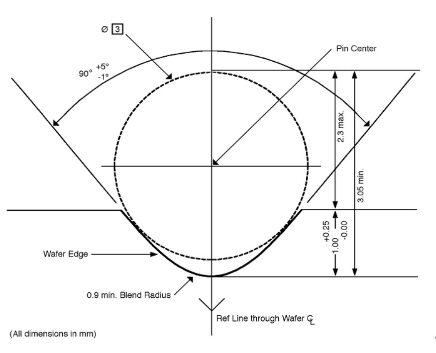
| 자투리 | 최대 7도 |
| 입자 | <10@0.5um、<10@0.3um、 <10@0.2um |
기술적 장점
Sub-nm Surface Precision:Ultra-smooth DSP (Double-Side Polished) surfaces with Ra <0.2nm, certified by AFM metrology, enabling defect-free EUV lithography for 3nm GAA transistor patterning.
Industry-Leading Defect Control:COP (Crystal Originated Pit) density <5/cm² on 300mm Prime wafers, achieving 99.98% yield in 3D NAND vertical stacking processes.
Thermal Stability Mastery:Oxygen content stabilized at 8-12ppma (±0.5ppma) via CZ/FZ crystal growth, minimizing wafer warpage <0.5μm under 1000°C epitaxial deposition.
Future-Ready Compatibility:300mm wafers with ≤2mm edge exclusion zone, fully compatible with 450mm fab automation interfaces for hybrid production lines.
Cost-Smart Sustainability:Reclaimed 200mm wafers reduce COO (Cost of Ownership) by 45% while maintaining ≤25 particles/addon (>0.2μm) for PMIC and analog IC production.
Doping Precision Engineered:Resistivity uniformity ±1% across 300mm wafers, supporting 0.001-10000 Ω·cm ranges for GaN-on-Si and SiC hybrid power devices.
Zero-Contamination Assurance:Class 1 cleanroom packaging with <0.3ppb metal contamination (Cu/Fe/Al), validated by GD-MS and TXRF analysis.