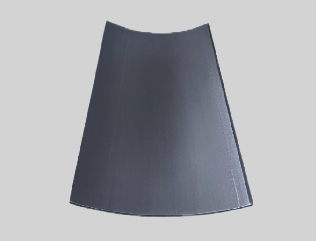
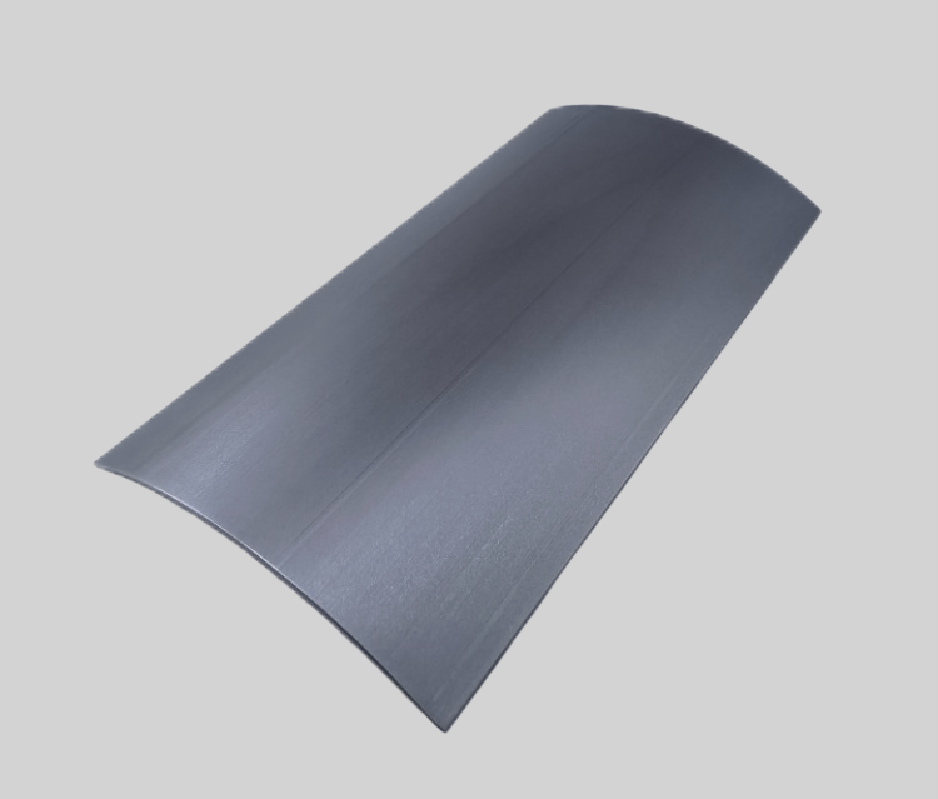
Ultra-Precise 3D Geometry Control:Achieve complex shapes (arcs, micro-cavities, tile patterns) via advanced lithography and anisotropic etching, enabling seamless integration into compact, high-density microdevices.
Stress-Engineered Structural Integrity:Proprietary stress-relief technology minimizes mechanical deformation during shaping, ensuring stability for quantum computing modules and aerospace-grade sensors.
Enhanced Signal Performance in RF & Optical Systems:Curved surfaces reduce signal loss in high-frequency RF circuits and improve light coupling efficiency for optical waveguides and photonic chips.
Customizable Surface Microstructures:Tailor micro-grooves, nano-patterns, or textured edges to optimize functionality in MEMS actuators, lab-on-a-chip devices, and biomedical implants.
High Thermal and Chemical Resistance:Maintain performance under extreme environments (e.g., high-temperature semiconductor processes or corrosive medical diagnostics).