
실리콘 소재를 위한 원스톱 솔루션 제공
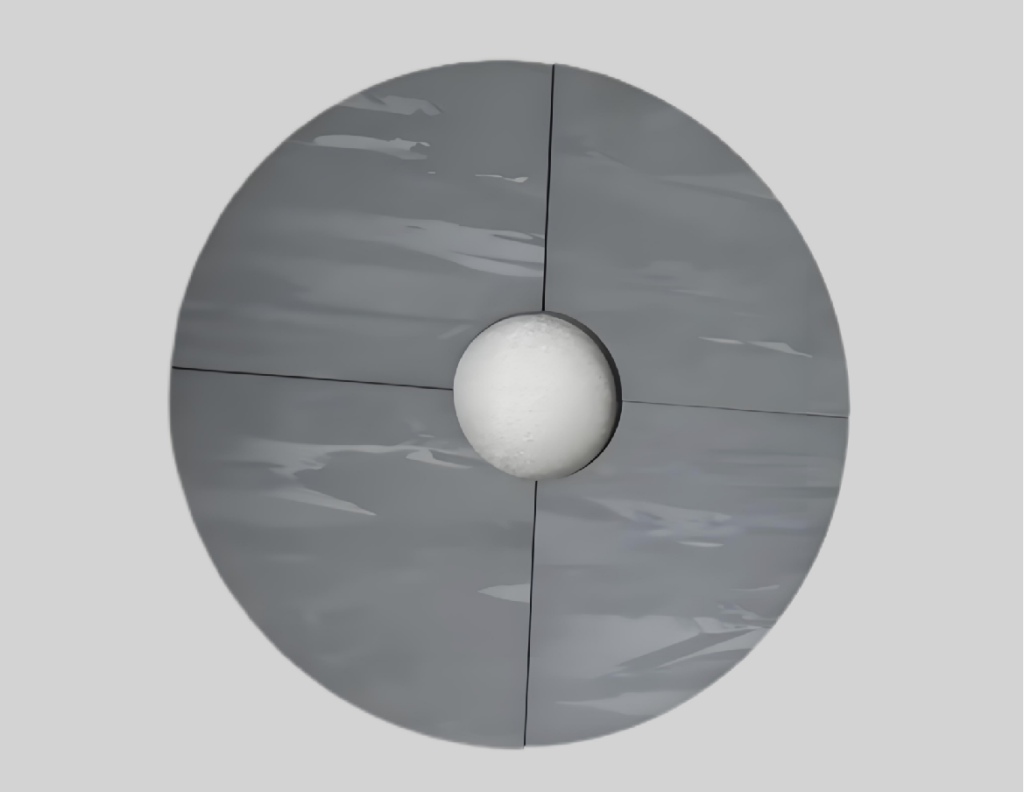
Silicon Custom-shaped Sputtering Targets are specialized materials designed for advanced thin-film deposition requiring non-conventional geometries. These targets include U-shaped, polygonal, semi-circular, and arc-shaped profiles, enabling precise coating of complex components in semiconductor, optical, and aerospace applications. Monocrystalline Silicon Targets deliver ultra-high purity (99.9999%) for nanoscale electronics, while Polycrystalline Silicon Variants offer cost-effective solutions for large-area coatings. Engineered for seamless integration with PVD/CVD systems, these targets support tailored resistivity, thermal stability, and edge-to-edge uniformity, meeting the demands of MEMS sensors, quantum devices, and high-efficiency solar cells.
기술 사양
| 아니요. | 특징 | 단위 | 사양 |
|---|---|---|---|
| 1 | 순수함 | % | >6N |
| 2 | 재료 | / | 모노 / 폴리 |
| 3 | 직경 눈금 | 음 | 0~2000 / Customizable |
| 4 | 유형/포함 사항 | / | P형/ N형 |
| 5 | 저항률 | Ω·cm³ | <0.02 / 1~4 / 60~90 |
| 6 | 결정 방향 | / | (100), (111), (110) |
| 7 | 도판트 | / | B, P, Ga, As, Sb |
| 8 | Ra | um | ≤0.8 |
기술적 장점
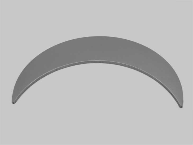
Multi-Profile Flexibility (U-shape, Polygon, Arc, etc.):Coat complex 3D components seamlessly with U-shaped, polygonal, or semi-circular silicon targets, eliminating edge gaps in MEMS and optical device fabrication.
Ultra-High Purity (99.9999%) for Nanoscale Precision:Ensure defect-free thin films in quantum computing and advanced ICs using monocrystalline silicon custom geometries, certified for ISO Class 2 cleanrooms.
Thermal Stability in High-Power Sputtering:Maintain consistent deposition rates with crystalline silicon’s superior heat dissipation, reducing thermal warping by 25% versus standard alloys.
Material Efficiency via Tailored Geometry:Reduce raw material waste by 40% through non-standard target designs, optimized for curved aerospace components or microfluidic chip coatings.
Edge-to-Edge Uniformity (<1% Thickness Variation):Achieve flawless coatings on irregular surfaces with arc-shaped or polygonal targets, critical for high-efficiency solar cells and wear-resistant layers.
Dual-Process Compatibility (PVD & CVD):Accelerate R&D-to-production workflows with multi-system adaptable silicon targets, supporting both ion beam sputtering and plasma-enhanced CVD.
Rapid Prototyping for Niche Applications:From lab-scale prototypes to industrial-grade batches, deliver custom geometries (e.g., hexagonal, semi-annular) in 4-6 weeks for R&D in photonics or flexible electronics.