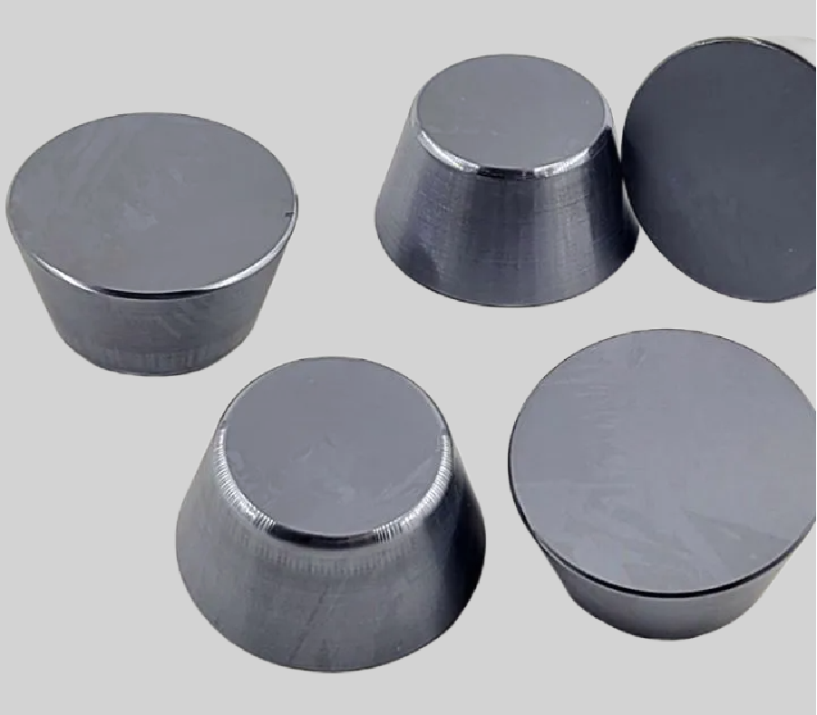
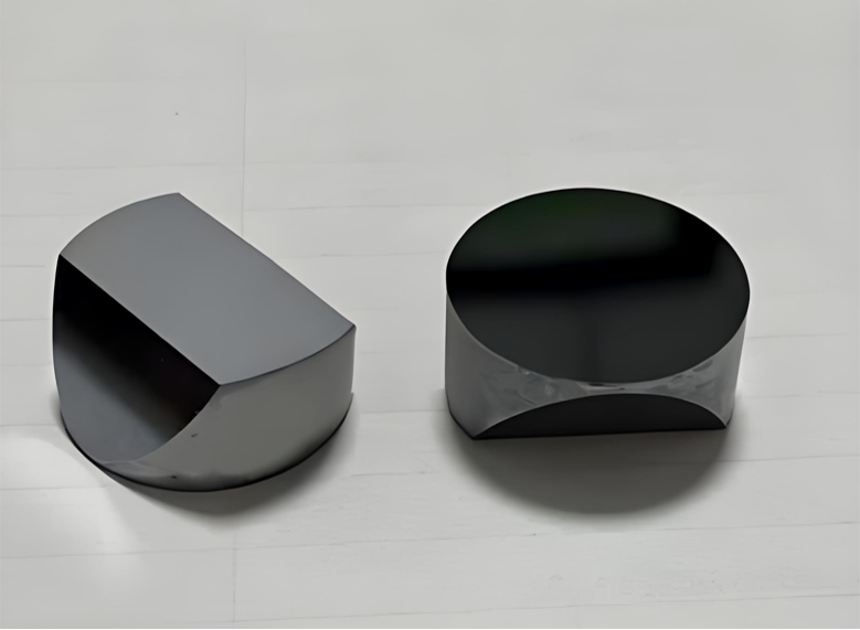
Submicron Geometric Accuracy (<±0.2μm) with Multi-axis Diamond Tooling:Achieve complex 3D shapes (prisms, hexagons, waveguides) while preserving crystal lattice integrity.
Semiconductor-Grade Material Compliance (6N+ Purity, ASTM F57):Guaranteed <0.01ppb metallic impurities for quantum computing and hyperspectral optics applications.
Non-Destructive Edge Profiling via Laser Shock Peening:Create chamfers/radii down to 50μm without microfractures, critical for MEMS membrane durability.
Crystal Orientation-Aligned Machining (XRD Verified):Precision alignment to <100>, <110>, or <111> planes with 0.5° angular tolerance for epitaxial growth.
CTE-Matched Hybrid Bonding Surfaces:Ultra-flat interfaces (Ra<0.1nm) engineered for direct fusion with Si,or sapphire substrates.
In-situ Metrology-Enabled Adaptive Processing:Real-time Raman spectroscopy feedback adjusts machining parameters to prevent phase transformation.
Vacuum-Compatible Geometric Stability:Maintain dimensional tolerance <5ppm under 10^-9 Torr environments, ideal for space-grade sensors.