
실리콘 소재를 위한 원스톱 솔루션 제공
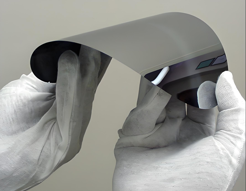
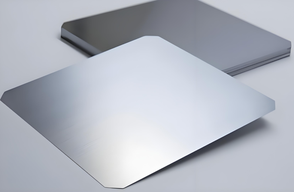
맞춤형 실리콘 웨이퍼는 첨단 반도체, 태양광, MEMS 응용 분야의 정밀한 기술적 요구 사항을 충족하도록 설계되었습니다. 이 웨이퍼는 특정 소자의 전기적 성능을 최적화하기 위해 맞춤형 저항률 수준(낮은 수준부터 높은 수준까지)을 제공합니다. 두께 맞춤화(초박형 50μm부터 표준 750μm+까지)를 통해 기계적 및 열적 요구 사항과의 호환성을 보장합니다. 기존의 원형 형식을 넘어, 제조업체들은 공간 효율적인 설계를 위한 직사각형 실리콘 웨이퍼와 생산 확장성을 높이기 위한 초대형 직경 웨이퍼(최대 450mm)를 포함한 독특한 치수 옵션을 제공합니다. 표면 마감, 결정 배향 및 가장자리 프로파일도 조정할 수 있어, 맞춤형 웨이퍼는 특수 센서, 전력 전자 장치 및 최첨단 광전자 시스템에 이상적입니다.
- Resistivity Control: Tailored from 0.01 to 10,000 Ω-cm using advanced doping techniques (e.g., boron/phosphorus), ensuring optimal performance for logic, analog/RF, or high-voltage devices.
- Thickness Flexibility: From ultra-thin 10μm membranes for MEMS and photonics to 12mm thick substrates for power electronics, with tight tolerances down to ±1μm.
- Size & Shape Innovation: Rectangular formats (e.g., 500*500mm) and industry-leading 450mm diameters, maximizing material efficiency and reducing per-chip costs.
기술 사양
| 프로젝트 | 내용 |
|---|---|
| 직경 | 2"(50.8mm), 3"(76.2mm), 4"(100mm), 5"(125mm), 6"(150mm), 8"(200mm), 12"(300mm) |
| 등급 | Prime, Test, Dummy, Reclaimed |
| 성장 방법 | CZ, FZ |
| 오리엔테이션 | 100 , 111 , 110 |
| 유형/도핑제 | P형/붕소, N형/인, N형/비소, N형/안티몬 |
| 저항률 | 0.001에서 10,000 옴·cm까지 |
| 두께 (μm) | 50~3000μm |
| 두께 공차 | 표준 ± 25μm, 최대 정밀도 ± 5μm |
| TTV (μm) | Standard < 10 um、Maximum Capabilities <5 um |
| 보/워프 (μm) | Standard <40 um、Maximum Capabilities <20 um |
| 완료 | 절단, 래핑, 에칭, SSP, DSP 등 |
| 자투리 | 최대 7도 |
| 입자 | <10@0.5um、<10@0.3um、 <10@0.2um |
기술적 장점
1. Precision Parameter Control for Mission-Critical Demands
- Tailored resistivity range from 0.001Ω·cm to 10,000Ω·cm, with flexible doping type (P/N) and concentration adjustments to meet diverse electrical requirements for power devices, sensors, and more.
- Thickness customization from ultra-thin 50μm to standard 1000μm, optimized for chip thinning, thermal management, or mechanical robustness.
2. Non-Standard Dimensions & Shapes to Unlock Innovation
- Deliver rectangular, trapezoidal, or ultra-large diameter (450mm+) silicon wafers, enabling compact integration or high-throughput manufacturing while minimizing material waste.
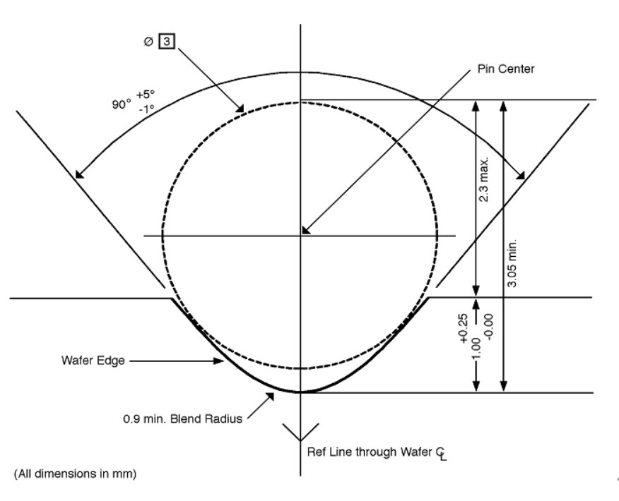
- Custom edge profiles (e.g., Notch, Flat) to enhance wafer processing compatibility and yield rates.
3. End-to-End Collaborative Development for Rapid Solutions
- Provide turnkey solutions covering crystal orientation selection (<100>/<111>/SOI), surface finishes (polished/textured), and wafer-level packaging.
- Leverage AI-driven simulation modeling + real-world testing feedback to reduce custom product development cycles by over 30%.
4. Rigorous Quality Assurance for Unmatched Consistency
- Implement laser-scanned resistivity mapping and nanoscale thickness uniformity inspection, ensuring critical parameter tolerances within ±1%