
실리콘 소재를 위한 원스톱 솔루션 제공
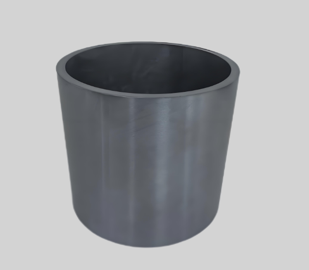
- Ultra-Precision Machining: Available in inner diameters from 1mm to 600mm with dimensional tolerances within ±0.05mm, suitable for tight-fit installations in diffusion furnaces or plasma chambers.
- High-Temperature Performance: Withstand prolonged exposure to 1200°C in oxidizing atmospheres, outperforming quartz tubes in extreme thermal cycling scenarios.
- Purity Assurance: Manufactured in ISO 8 cleanrooms to minimize particle contamination, meeting SEMI standards for semiconductor-grade components.
- Customization Options: Polished inner/outer surfaces, flanged ends, or integrated gas distribution holes for tailored applications in MEMS device fabrication or nuclear radiation detection.
기술 사양
| 아니요. | 특징 | 단위 | 사양 |
|---|---|---|---|
| 1 | 순수함 | % | >9N |
| 2 | 재료 | / | 모노 |
| 3 | 직경 눈금 | 음 | 0~1000 / 사용자 정의 가능 |
| 4 | 유형/포함 사항 | / | P형/ N형 |
| 5 | 저항률 | Ω·cm³ | <0.02 / 1~4 / 60~90 |
| 6 | 결정 방향 | / | (100), (111), (110) |
| 7 | 작동 온도 | ℃ | <1250 ℃ |
| 8 | 길이 | 음 | 50~2000 |
기술적 장점
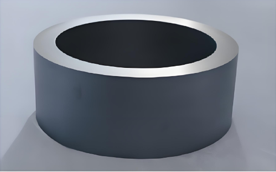
Ultra-High Purity & Low Defect Density:Manufactured from electronic-grade single crystal silicon (9N purity) with impurity levels below 0.1 ppb, ensuring zero contamination in semiconductor processes and significantly improving wafer yield.
Exceptional Thermal Stability:Withstands extreme temperatures up to 1,250°C, featuring ultra-low thermal expansion coefficient (≈3×10⁻⁶/°C) and superior thermal shock resistance, ideal for rapid temperature cycling in oxidation, diffusion, and LPCVD processes.
Chemical Inertness for Process Integrity:Grain boundary-free surface eliminates side reactions with aggressive gases (e.g., Cl₂, HCl, H₂), preventing particle shedding and ensuring film uniformity (thickness variation < ±2%).
Extended Lifespan & Reduced Maintenance:Monocrystalline structure delivers outstanding creep resistance, with a service life exceeding 5,000 hours under continuous high-temperature operation, reducing downtime costs by 30%.
Compatibility with Advanced Nodes:Supports sub-3nm process technologies, meeting stringent cleanliness requirements for EUV lithography and High-k dielectric deposition, enabling mass production of cutting-edge chips.
Precise Thermal Field Control:Thermal conductivity (≈150 W/m·K) closely matches quartz, achieving furnace temperature gradients ≤1°C/cm for uniform wafer doping (RSD < 3%).
Sustainability Alignment:Compliant with SEMI F47 standards, compatible with hydrogen-based and low-carbon processes (e.g., SiH₄-Cl₂ gas mixtures), supporting semiconductor industry carbon neutrality goals.