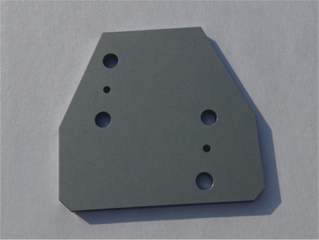
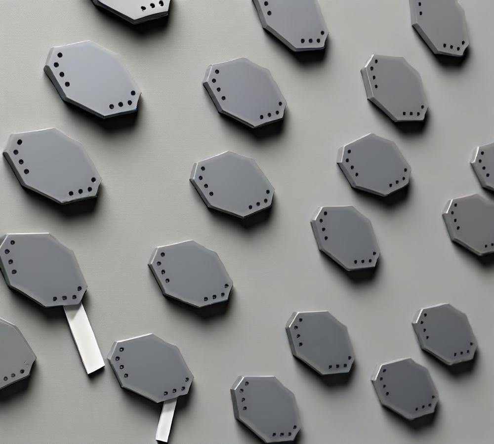
Advanced Laser Drilling Technology:Achieve micron-level precision with minimal thermal damage, ensuring flawless micro-hole patterns for critical applications.
Micron-Level Accuracy for High-Density Arrays:Consistent hole diameters (from 5µm to 50mm) , ideal for MEMS, photonics, and sensor integration.
Superior Material Integrity:High-purity monocrystalline silicon substrates maintain exceptional thermal stability (up to 1200°C) and electrical performance.
Custom Design Flexibility:Tailor hole geometry, pitch, and patterns (hexagonal, radial, or random) to meet your unique R&D or production requirements.
Multi-Layer Compatibility:Seamlessly integrate with thin-film coatings, metallization, and hybrid bonding processes for advanced semiconductor devices.
Rapid Prototyping & Scalable Production:From small-batch R&D samples to high-volume orders, deliver industry-leading turnaround times without compromising quality.
Enabling Next-Gen Innovations:Power breakthroughs in quantum computing, microfluidics, and optical systems with ultra-precise perforated silicon solutions.