
실리콘 소재를 위한 원스톱 솔루션 제공
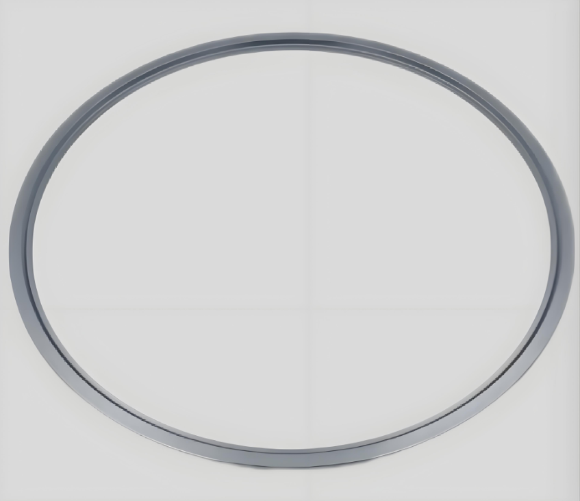
- Plasma Confinement: By generating an electric field around the wafer perimeter, silicon focus rings direct plasma ions toward the target area, reducing etch non-uniformity caused by plasma diffusion.
- Edge Protection: Their concave or stepped design shields the wafer’s edge from excessive plasma bombardment, preventing damage during high-energy etching.
- Material Compatibility: High-purity silicon variants resist corrosion from fluorine-based etchants (e.g., SF₆), while SiC-coated rings withstand extreme temperatures (up to 1400°C) and corrosive environments.
- Customization: Available in diameters from 8″ to 12″ (200–300mm), with options like vacuum channels for secure wafer clamping and anti-static surfaces to mitigate particle contamination.
기술 사양
| 아니요. | 특징 | 단위 | 사양 |
|---|---|---|---|
| 1 | 순수함 | % | >6N |
| 2 | 재료 | / | 모노 / 폴리 |
| 3 | 직경 눈금 | 음 | 0~500 / Customizable |
| 4 | 유형/포함 사항 | / | P type / N type |
| 5 | 저항률 | Ω·cm³ | <0.02 / 1~4 / 60~90 |
| 6 | 결정 방향 | / | (100), (111), (110) |
| 7 | 도판트 | / | B, P, Ga, As, Sb |
| 8 | 표면 처리 | / | 연마 |
기술적 장점
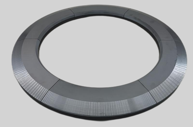
High-Purity Silicon (99.99999%):Engineered with contamination-free material to eliminate wafer edge defects in ultra-sensitive EUV and high-k dielectric etching processes.
Extreme Plasma & Chemical Resistance:Withstands corrosive plasmas (Cl₂, O₂, HBr) and thermal cycling up to 750°C, ensuring 20,000+ process cycles without degradation.
Edge Etch Uniformity Control:Precision-machined geometry reduces edge exclusion zones to <1mm and achieves ±1% etch rate uniformity across 300mm wafers.
Multi-Frequency RF Compatibility:Optimized dielectric properties ensure stable plasma coupling under 2MHz-60MHz RF ranges, critical for advanced 3D NAND and GAA transistor fabrication.
Low-Particle Surface (Ra <0.2nm):Atomic-level polishing minimizes micro-arcing and particle adhesion, improving overall wafer yield to >99.97%.