실리콘 소재를 위한 원스톱 솔루션 제공

Home / Products / Si Shaped / Silicon Seed Crystal

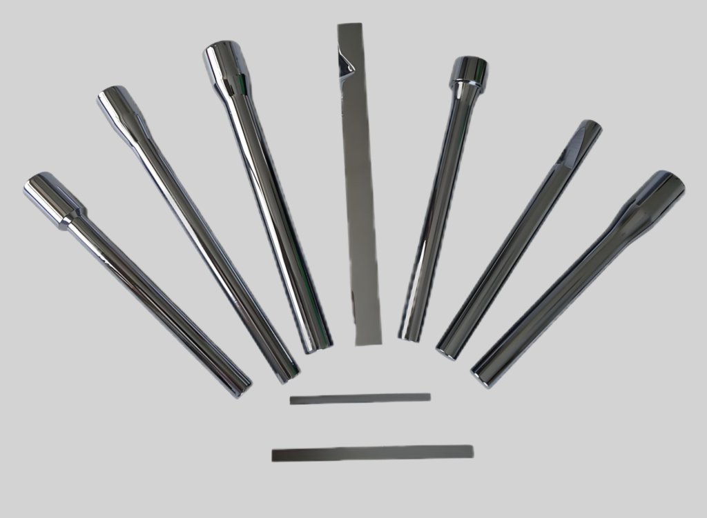
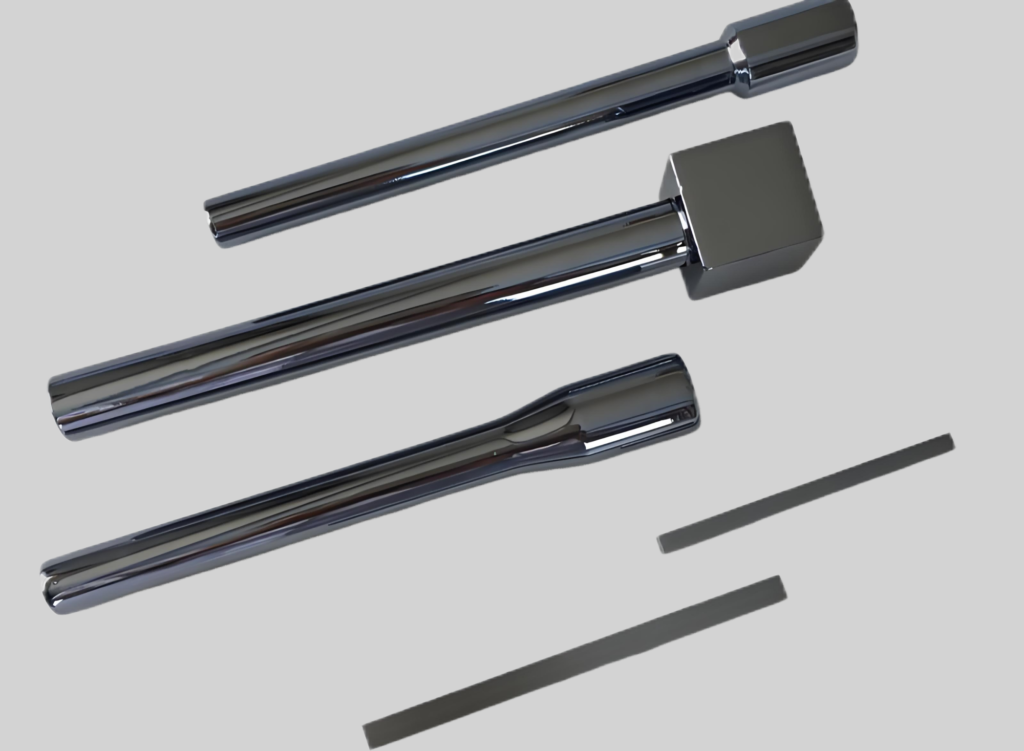
실리콘 성장용 시드 크리스탈
A silicon seed crystal is a high-purity, single-crystal silicon rod used as the foundation for growing larger monocrystalline silicon ingots through the Czochralski (CZ) process . This process involves dipping a precisely oriented seed crystal into molten silicon and slowly pulling it upward while rotating, resulting in a cylindrical ingot with uniform crystallinity Silicon seed crystals are critical in semiconductor manufacturing, where they enable the production of wafers for microchips, power devices, and solar cells.
  • Ultra-high purity (up to 11N, 99.999999999%) to ensure electronic performance .
  • Doping capabilities (e.g., boron for p-type or phosphorus for n-type) to tailor conductivity .
  • Precision diameters (e.g., 200mm/300mm) to meet industry standards for wafer fabrication.

기술 사양

아니요.특징단위사양
1순수함%>6N/9N
2재료/모노
3직경 눈금0~300 / Customizable
4유형/포함 사항/P형/ N형
5저항률Ω·cm³<0.02 / 1~4 / 60~90
6결정 방향/(100), (111), (110)
7제품 길이1~300
8표면 처리/연마
CZ silicon seed crystal (Czochralski process)

기술적 장점

  1. Ultra-High Purity & Structural Integrity:Ensures uniform lattice alignment for defect-free monocrystalline silicon growth, critical for high-performance semiconductors and solar cells.

  2. Precision Crystallographic Orientation Control:Customizable orientations (e.g., <100>, <111>) to optimize electrical properties and device efficiency in targeted applications.

  3. Enhanced Yield in Czochralski (CZ) Process:Minimizes thermal stress and dislocation defects, enabling faster production of high-quality silicon ingots with reduced material waste.

  4. Long-Term Thermal Stability:Maintains structural integrity under extreme temperatures, supporting reliable crystal growth for industrial-scale manufacturing.

  5. Versatility Across Industries:Compatible with semiconductor fabrication, photovoltaic systems, and advanced electronics, ensuring broad applicability.

  6. Advanced Surface Polishing Technology:Ultra-smooth seed surfaces reduce nucleation errors, accelerating consistent crystal replication.