
실리콘 소재를 위한 원스톱 솔루션 제공
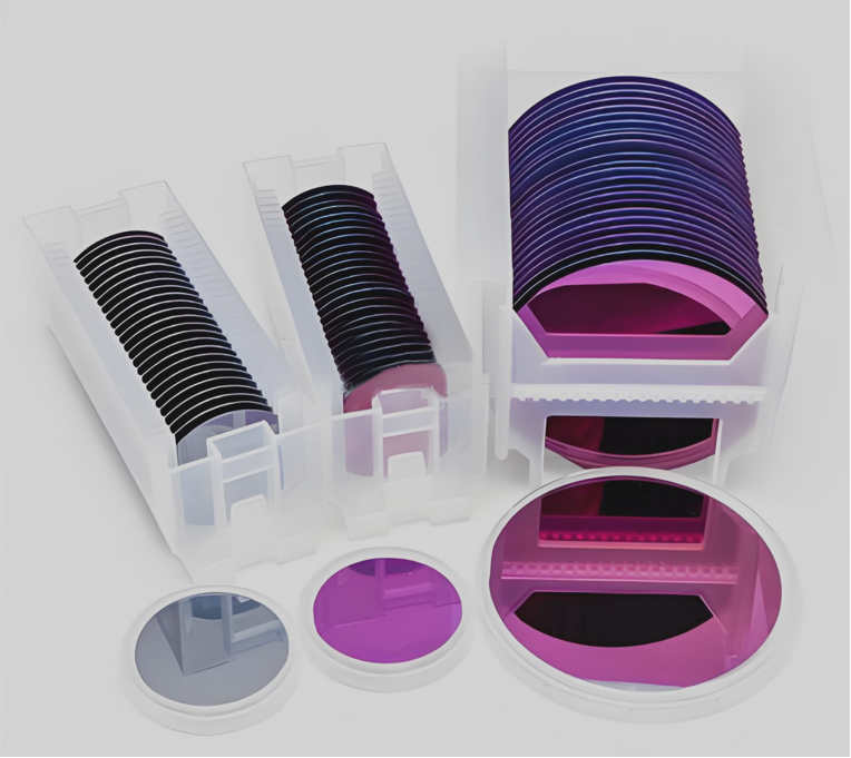
- High dielectric strength (up to 10 MV/cm) for reliable insulation.
- Uniform thickness control (ranging from nanometers to micrometers) via dry or wet oxidation processes.
- Chemical inertness and resistance to harsh etching environments.
기술 사양
| 프로젝트 | 내용 |
|---|---|
| 직경 | 2"(50.8mm), 3"(76.2mm), 4"(100mm), 5"(125mm), 6"(150mm), 8"(200mm), 12"(300mm) |
| 등급 | Prime, Test, Dummy, Reclaimed |
| Oxidation Technique | Wet oxidation or Dry oxidation |
| Oxide Thickness | 100 Å ~ 15µm |
| Tolerance | +/- 5% |
| Surface | Single Side Oxidation(SSO) / Double Sides Oxidation(DSO) |
| Furnace | Horizontal tube furnace |
| Gas | Hydrogen and Oxygen gas |
| Temperature | 900℃ ~ 1200 ℃ |
| Refractive index | 1.456 |
기술적 장점
Ultra-High Purity & Uniformity: Our silicon oxide wafers (SiO₂) are engineered with 99.999999% purity, ensuring minimal defects and exceptional uniformity for precise semiconductor fabrication and MEMS applications.
Superior Thermal Stability: Withstanding extreme temperatures up to 1200°C, our SiO₂ wafers maintain structural integrity in high-temperature processes like thermal oxidation and CVD, critical for advanced IC manufacturing.
Optimal Dielectric Performance: Featuring high dielectric strength (>10 MV/cm), our oxide layers enable efficient electrical insulation, reducing leakage currents and enhancing device reliability in microelectronics and power semiconductors.
Chemically Inert Surface: The inert nature of our SiO₂ wafers resists corrosion from acids, bases, and plasma, ideal for harsh etching environments and long-term stability in MEMS and optoelectronic devices.
Nanoscale Precision: Customizable oxide thickness (1nm to 2µm) and ultra-smooth surface roughness (<0.5nm RMS) support cutting-edge nanotechnology, photolithography, and quantum device research.
Versatile Integration: Compatible with silicon substrates and standard CMOS/MEMS processes, our wafers streamline production of sensors, optical coatings, and gate oxides, accelerating time-to-market.
Eco-Friendly Durability: Engineered for high environmental resistance (moisture, UV, oxidation), our SiO₂ wafers extend product lifespans in aerospace, automotive, and renewable energy systems.