Choosing between single-side polished (SSP) and double-side polished (DSP) silicon wafers is not simply a matter of process preference—it is an engineering decision determined jointly by device structure, process requirements, and cost-effectiveness. The core difference is: SSP is the economical choice of “good enough,” while DSP is the performance choice of “ultimate flatness.”
SSP: Only the front side is polished to very high surface quality.
DSP: Both front and back sides must achieve high flatness/surface quality.
The key is not “which one is more advanced,” but whether subsequent processes actually require the backside to be good enough.
1. Why Is SSP Sufficient?
Typical structure:
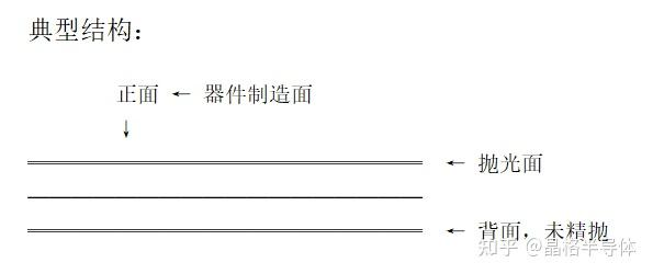
If subsequent processes use almost exclusively the front side, then polishing only the front side is enough.
For example:
- Silicon wafers for general ICs
- Some discrete devices
- Power devices
- Products with lower requirements for backside flatness
In such cases, polishing the backside as well would increase:
- Process cost
- Processing time
- Silicon wafer loss
- Cleaning difficulty
So it is unnecessary.
2. Why Does DSP Need to Polish the Backside Too?
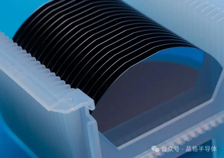
DSP: Both sides are polished.
Its greatest value is not simply “a smoother backside,” but achieving better:
- Flatness and geometry control.
For example:
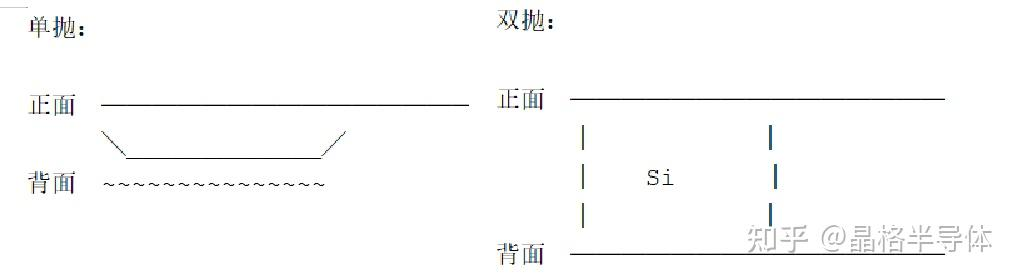
After DSP, the geometric state of both wafer surfaces is easier to control, making it especially suitable for applications with high requirements for thickness uniformity, warpage, and flatness.
3. A Very Important Distinction: Is the Backside Also a “Process Surface”?
This is actually the core criterion for judging SSP vs. DSP.
For example, in certain processes:
Front side:
- Photolithography
- Etching
- Thin film deposition
- Ion implantation
Backside:
- Also requires photolithography/alignment
- Requires bonding
- Requires epitaxy
- Requires high-precision measurement
- Needs to serve as a mechanical/optical reference surface
Then the backside quality cannot be too poor, so DSP is preferred.
4. Trade-off Between Performance and Cost
The performance differences between the two processes directly determine their application areas.
| Characteristic | Single-Side Polished (SSP) | Double-Side Polished (DSP) |
|---|---|---|
| Surface quality | Only front side reaches mirror grade (roughness <0.5 nm); backside roughness is 1–2 orders of magnitude higher | Both sides reach mirror grade (roughness typically <0.5 nm); extremely few surface defects |
| Flatness | Relatively poorer plane parallelism | Better global flatness; excellent thickness uniformity |
| Mechanical strength | Higher; retains original backside structure, strong fracture resistance | Slightly lower; material removed from both sides reduces strength by about 10%–15% |
| Processing cost | Lower; simple process, short cycle | Higher; complex process, requires symmetry in both-side treatment |
5. Application Scenarios: How to Choose?
Typical applications of SSP silicon wafers
When devices need to be built only on the front side, and the backside serves merely as mechanical support and a heat conduction path, SSP is the cost-effective choice.
- Traditional CMOS integrated circuits: All devices are fabricated on the front side; the backside only needs to ensure mechanical strength.
- Basic MEMS devices: Such as pressure sensors, accelerometers, microfluidic devices, and micromirrors. These devices usually require only front-side processing.
- Power devices requiring backside thinning or metallization: Retaining the original backside facilitates subsequent thinning and metallization processes.
Typical applications of DSP silicon wafers
When device manufacturing requires processing on both sides of the wafer, or when there are extreme requirements for global flatness, DSP wafers must be used.
- 3D ICs and advanced packaging: Such as through-silicon via (TSV) technology, which requires photolithography and etching from both sides of the wafer. DSP ensures alignment accuracy and consistency.
- Wafer bonding: DSP wafers have mirror-grade surfaces on both sides, providing excellent bonding strength and sealing performance—ideal for MEMS cap wafers.
- High-performance MEMS devices: Such as advanced inertial sensors (gyroscopes), resonators, and optical MEMS. These devices often require double-side photolithography or extremely high flatness.
- High-voltage power semiconductors and RF devices: Strict requirements for global flatness and thickness uniformity make DSP the standard configuration.
- Scenarios requiring ultra-thin wafers: In advanced packaging, wafers must be thinned to below 100 μm. DSP provides better initial flatness to ensure reliability in subsequent processing.
Article source: Jingge Semiconductor — Supplies ultra‑large‑size single‑crystal silicon materials and polycrystalline columnar‑grained silicon materials. Our products are specifically designed for the processing of silicon components used in semiconductor etching applications, including single‑crystal silicon rings, single‑crystal silicon wafers, columnar‑grained silicon rings, and polycrystalline silicon wafers, with diameters up to 650 mm.