⚡ One-Sentence Core Conclusion
The “etch-stop” phenomenon of heavily boron-doped silicon in alkaline solutions is fundamentally an electrical effect dominated by high concentrations of holes, rather than simple chemical bond strengthening. When the boron concentration exceeds a critical threshold, the electrochemical state of the silicon surface undergoes a fundamental change, cutting off the electron supply required for the dissolution reaction.
📊 Key Parameters at a Glance
Threshold Concentration: Approximately 2×10¹⁹ cm⁻³, corresponding to the onset of degeneracy in p-type silicon, where the Fermi level drops into the valence band and the material begins to exhibit metal-like electrical behavior.
Effective Working Concentration: Above 5×10¹⁹ cm⁻³, where the etch rate drops to below 1/100 of that of lightly doped silicon.
Rate-Concentration Relationship: The etch rate decreases inversely with the fourth power of boron concentration.
Core Mechanism: Electrical effect — high hole concentration consumes electrons required for the dissolution reaction, the space charge layer collapses, and electron tunneling–Auger recombination occurs.
Auxiliary Mechanism: In-situ formation of an ultra-thin SiOx passivation layer further impedes etching.
Typical Application: Etch-stop layers in MEMS micromachining, KOH/EDP anisotropic etching.
❓ What Is the “Etch-Stop” Phenomenon of Heavily Boron-Doped Silicon?
Answer: When the boron doping concentration in silicon exceeds approximately 2×10¹⁹ cm⁻³, its dissolution rate in alkaline anisotropic etchants such as potassium hydroxide (KOH) and ethylenediamine-pyrocatechol (EDP) drops sharply, almost to a halt. This phenomenon is known as “etch-stop.”
In silicon micromachining, engineers exploit this property by using heavily boron-doped layers as etch-stop layers, precisely controlling the depth and shape of structures during subsequent alkaline etching to fabricate three-dimensional structures such as micro-holes, cantilevers, and thin films.

❓ What Is the Threshold Concentration for Etch-Stop?
Answer: The threshold concentration is approximately 2×10¹⁹ cm⁻³.
Numerous studies consistently show that when the boron concentration exceeds this level, the etch rate begins to decrease significantly. This threshold precisely corresponds to the onset of “degeneracy” in p-type silicon — when the boron concentration reaches this level, the Fermi level of silicon drops into the valence band, and the material begins to exhibit metal-like characteristics in its electrical behavior.
In engineering practice, heavily boron-doped layers with concentrations above 5×10¹⁹ cm⁻³ are typically used to achieve effective etch-stop. When the boron concentration reaches the order of 10²⁰ cm⁻³, the etch rate can drop to below 1/100 of that of lightly doped silicon.
❓ What Is the Core Mechanism of Etch-Stop?
Answer: The core mechanism is an electrical effect, not simple chemical bond strengthening.
In normal alkaline etching, silicon dissolution is an electrochemical process: silicon atoms are oxidized, releasing electrons into the conduction band; simultaneously, water molecules are reduced, producing hydroxide ions (OH⁻). These electrons injected into the conduction band need to temporarily remain near the silicon surface to effectively participate in subsequent reduction reactions and drive etching forward.

In heavily boron-doped silicon, however, the high concentration of holes completely changes this situation:
1. Sharp contraction of the space charge layer. High doping concentration causes the width of the space charge layer at the silicon surface to shrink dramatically. In the degenerate state, band bending is confined to an extremely thin region of only about one atomic layer. The potential well that could originally “trap” electrons almost disappears.
2. Electron tunneling and Auger recombination. Electrons injected into the conduction band by the oxidation reaction can no longer be confined to the surface. They can directly tunnel through this extremely narrow barrier into the bulk of the p++ silicon and rapidly recombine with the abundant holes in the valence band.
3. Dissolution reaction interruption. Since the electrons required for the water molecule reduction reaction are largely consumed, the silicon surface cannot continuously generate new hydroxide ions. Without hydroxide ions, the silicon dissolution reaction loses its driving force, and the etching process stalls.
This electrical model is strongly supported by a key experimental observation: the reduction in etch rate is inversely proportional to the fourth power of boron concentration. The reason is that dissolving one silicon atom requires the transfer of four electrons. In the etch-stop regime, the residual etch rate depends on the extremely small number of un-recombined electrons in the conduction band, and the number of these electrons is inversely proportional to the hole (i.e., boron) concentration. Therefore, the fourth-power dependence of etch rate on boron concentration perfectly corresponds to the stoichiometric requirement that “one silicon atom requires four electrons,” providing quantitative evidence for the electrical model.
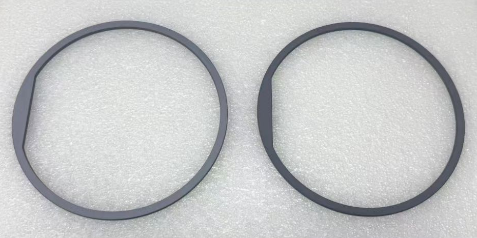
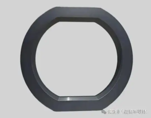
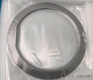
Jingge Semiconductor supplies ultra-large-size single-crystal silicon materials and polycrystalline columnar-grained silicon materials. Products are suitable for processing silicon components used in semiconductor etching, including single-crystal silicon rings, single-crystal silicon wafers, columnar-grained silicon rings, and polycrystalline silicon wafers, with diameters up to 650 mm.
❓ Are There Other Mechanisms Beyond the Electrical Effect?
Answer: Yes. Some studies have also observed an auxiliary role of a surface passivation layer.
On the surface of heavily boron-doped silicon, an ultra-thin SiOx (silicon oxide) passivation layer forms in situ. This oxide layer further impedes the etching reaction, acting as a physical barrier. High concentrations of holes promote the growth of this oxide layer, and lattice strain introduced by heavy doping may also enhance its density. Therefore, etch-stop may be the result of synergistic action between electron supply interruption and surface oxidation passivation.
📊 Key Factors Affecting Etch-Stop Effectiveness
The effectiveness of etch-stop is not constant; it is significantly influenced by the following factors:
Etchant type: The selectivity varies greatly among different alkaline etchants. For heavily boron-doped silicon, EDP and low-concentration KOH provide the best etch-stop effect, while high-concentration KOH is relatively weakest. TMAH also provides good selectivity with better safety. The etch rate ratio of undoped silicon to heavily boron-doped silicon can range from 10:1 to over 500:1 depending on the etchant.
Temperature: The temperature dependence of the critical boron concentration is related to the temperature dependence of the onset of degeneracy. At lower temperatures, the etch-stop effect is typically more pronounced.
Crystal orientation: The etch-stop effect exists on different crystal planes, but has been most extensively studied and applied on the (100) plane.
💎 Summary
The etch-stop effect of heavily boron-doped silicon can be summarized as follows:
One essence: An electrical effect, not chemical bond strengthening. High hole concentration alters the electrochemical state of the silicon surface.
One threshold: Approximately 2×10¹⁹ cm⁻³ boron concentration, corresponding to the onset of degeneracy.
One rule: Etch rate is inversely proportional to the fourth power of boron concentration, originating from the requirement to transfer four electrons to dissolve one silicon atom.
One auxiliary mechanism: In-situ formation of a SiOx passivation layer further impedes etching.
Final conclusion: The etch-stop effect of heavily boron-doped silicon provides a highly selective process tool for silicon micromachining. Understanding its electrical nature and quantitative laws is fundamental to precisely controlling the dimensions and shapes of MEMS structures.