⚡ One-Sentence Core Conclusion
Silicon components in plasma etching equipment — silicon electrodes, silicon rings, and showerheads — almost universally choose boron-doped P-type silicon because boron’s physical properties in silicon perfectly match the combined electrical, chemical, and mechanical requirements of the plasma etching environment. Boron has a high segregation coefficient (~0.8), enabling large-diameter single-crystal ingots with excellent resistivity uniformity; heavily boron-doped silicon exhibits lower sputtering yield and longer service life in plasma; and its “etch-stop” effect provides a critical process window for wet processing.
📊 Quick Overview of Boron-Doped Silicon’s Core Advantages
Natural advantage of P-type silicon: Boron’s segregation coefficient (~0.8) is far higher than that of phosphorus (~0.35), resulting in more uniform distribution during crystal growth and enabling large-diameter single-crystal ingots with excellent resistivity uniformity, which ensures symmetry of plasma distribution.
Precise resistivity control: The conductivity type of silicon rings for plasma etchers is explicitly specified as P-type boron-doped, with resistivity ranging from 0.02–85 Ω·cm. Boron doping concentration is typically controlled between 1×10¹⁸ and 1×10²⁰ atoms/cm³ — sufficient to uniformly conduct RF power without causing localized overheating due to excessively low resistivity.
Plasma erosion resistance: Heavily boron-doped silicon exhibits longer life and fewer particles in fluorine- or chlorine-based plasmas. Mechanisms include reduced sputtering yield, improved surface chemical stability, and uniform wear patterns.
Wet etch-stop effect: When boron concentration exceeds approximately 2×10¹⁹ cm⁻³, the etch rate of silicon in alkaline solutions such as KOH and TMAH drops sharply, providing a critical process control mechanism for fabricating micro-holes and micro-channels.
❓ Why Do Etching Silicon Components Almost Universally Choose P-Type Boron-Doped Silicon?
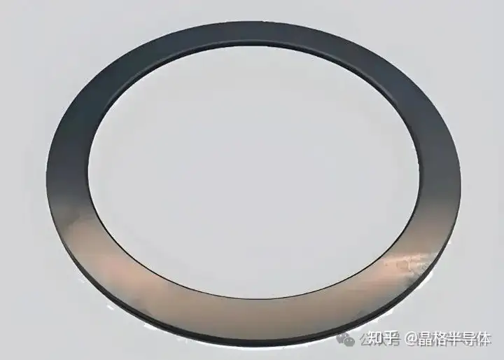
Answer: Etching silicon components (such as silicon electrodes, silicon rings, and showerheads) almost universally choose boron-doped P-type silicon. The reasons can be understood from three dimensions: electrical matching, plasma erosion resistance, and manufacturing process.
Reason 1: Natural Advantage of P-Type Silicon — High Segregation Coefficient
In semiconductor doping, boron (B) is the most commonly used Group III element for forming P-type silicon. Compared with phosphorus (N-type) doping, boron’s segregation coefficient in silicon (~0.8) is far higher than that of phosphorus (~0.35) . This means boron distributes more uniformly during crystal growth, making it easier to pull large-diameter single-crystal ingots with excellent resistivity uniformity.
Etching components typically require extremely high radial and axial resistivity uniformity to ensure symmetry of plasma distribution. If resistivity is non-uniform, RF current distribution becomes unbalanced, plasma density develops gradients, and ultimately the etch rate at the wafer edge differs from the center. Boron has an inherent advantage in this regard.
Reason 2: Precise Resistivity Control
The resistivity of etching silicon components is not chosen arbitrarily but follows strict standard ranges.
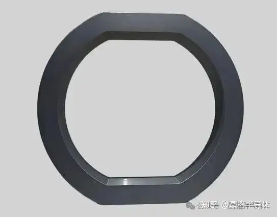
According to the group standard T/ZZB 3882—2024 “Silicon Rings for Plasma Etchers,” the conductivity type of silicon rings is explicitly specified as P-type boron-doped, with resistivity ranging from 0.02–85 Ω·cm, and radial resistivity variation percentage must be controlled. In patent literature, boron doping concentration for silicon components used in plasma etching equipment is typically controlled between 1×10¹⁸ and 1×10²⁰ atoms/cm³.
This concentration range enables precise tuning of silicon resistivity to a range suitable for RF coupling — ensuring sufficient conductivity to uniformly conduct RF power without causing localized overheating due to excessively low resistivity.
Reason 3: Erosion Resistance in Plasma Environments
Heavily boron-doped silicon exhibits longer life and fewer particles in fluorine- or chlorine-based plasma environments. The mechanisms mainly include three aspects:
Mechanism 1: Reduced sputtering yield. Lattice strain introduced by heavy boron doping alters the atomic binding energy of the silicon surface, reducing the physical sputtering yield under ion bombardment.
Mechanism 2: Improved surface chemical stability. Degenerate doping brings the silicon surface Fermi level into the valence band, altering charge exchange behavior between the surface and fluorine/chlorine radicals, potentially suppressing certain chemical etching pathways.
Mechanism 3: Uniform wear pattern. Heavily boron-doped silicon tends to be consumed in a “smooth wear” manner rather than forming pits through localized rapid erosion. This directly reduces particle generation and extends component life.
Reason 4: “Etch-Stop” Effect During Wet Processing
Silicon components require wet alkaline etching during the manufacturing stage to fabricate micro-holes, micro-channels, and other structures. Here, the “etch-stop” effect of heavily boron-doped silicon plays a critical role:
When boron concentration exceeds approximately 2×10¹⁹ cm⁻³, the etch rate of silicon in alkaline solutions such as KOH and TMAH drops sharply. The essence is an electrical effect: heavy boron doping brings silicon into a degenerate state, fundamentally changing the surface space charge layer and suppressing the chemical reaction pathway of alkaline etching.
❓ How Do Different Dopant Elements Compare?
Answer: The key differences between boron doping (P-type) and phosphorus doping (N-type) in etching silicon component applications are as follows:
Segregation coefficient: Boron ~0.8, far higher than phosphorus ~0.35; boron’s crystal growth uniformity is significantly superior to phosphorus.
Resistivity uniformity: Boron enables large-diameter single-crystal ingots with excellent resistivity uniformity; phosphorus uniformity is more difficult to control.
Wet etch-stop effect: Boron exhibits a significant etch-stop effect in KOH when concentration exceeds approximately 2×10¹⁹ cm⁻³; phosphorus has no such effect.
Plasma erosion resistance: Heavily boron-doped silicon exhibits reduced sputtering yield, improved surface chemical stability, and uniform wear patterns; N-type silicon has relatively insufficient erosion resistance under the same conditions.
Mainstream applications: Boron is the industry-standard dopant for etching silicon components (silicon rings, silicon electrodes, showerheads); phosphorus is mainly used for N-type device substrates and other applications.
❓ What Does This Mean for Material Selection in Etching Silicon Components?
Answer: The above mechanisms collectively determine the material selection logic for etching silicon components. Boron-doped silicon has become the industry standard essentially because it simultaneously satisfies requirements across electrical matching (resistivity uniformity), plasma erosion resistance (long life, low particles), and manufacturing process (etch-stop) — a combination that other doping types struggle to achieve.
For silicon component suppliers, this means controlling boron doping concentration and uniformity from the source of high-purity, large-size single-crystal silicon materials, while ensuring geometric precision and surface quality through precision machining, to meet the requirements of advanced nodes for etching uniformity and yield.
Jingge Semiconductor supplies ultra-large-size single-crystal silicon materials and polycrystalline columnar-grained silicon materials. Products are suitable for processing silicon components used in semiconductor etching, including single-crystal silicon rings, single-crystal silicon wafers, columnar-grained silicon rings, and polycrystalline silicon wafers, with diameters up to 650 mm.
💎 Summary
The core logic behind choosing boron-doped P-type silicon for etching silicon components can be summarized as follows:
One core: Boron’s physical properties (high segregation coefficient, precisely controllable resistivity) perfectly match the combined requirements of the plasma etching environment.
Four major advantages:
- High segregation coefficient (~0.8), excellent resistivity uniformity
- Precisely controllable resistivity range (0.02–85 Ω·cm)
- Strong plasma erosion resistance (low sputtering, uniform wear)
- Wet processing etch-stop effect
One key concentration threshold: When boron concentration exceeds approximately 2×10¹⁹ cm⁻³, a significant etch-stop effect occurs in alkaline solutions such as KOH — a critical process window for fabricating micro-holes and micro-channels.
Final conclusion: Boron-doped P-type silicon has become the standard material for etching silicon components not by coincidence, but as a result of the combined effects of boron’s segregation behavior, electrical properties, and chemical stability in silicon. Understanding this material selection logic is fundamental to optimizing etching processes and improving wafer yield.