One-Sentence Core Conclusion
The 775 μm thickness of a 300 mm silicon wafer is not derived from a simple formula based on diameter—it is the result of decades of engineering compromise among mechanical strength, wafer warpage, process compatibility, equipment handling, and material cost.
What Does “12-Inch” Actually Mean?
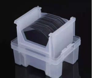
In the semiconductor industry, a “12-inch wafer” refers to a 300 mm diameter silicon wafer. The term “12-inch” is a historical imperial designation; 12 inches equals approximately 304.8 mm, but the industry-standard 300 mm wafer is not a strict conversion. For reference, 6-inch, 8-inch, and 12-inch wafers correspond to 150 mm, 200 mm, and 300 mm, respectively.
Critically, diameter and thickness are two independent parameters. The diameter determines how “large” the wafer is, while the thickness determines how “thick” it is. There is no simple mathematical relationship such as thickness = f(diameter).
Why Can’t Wafers Be Made Extremely Thin?
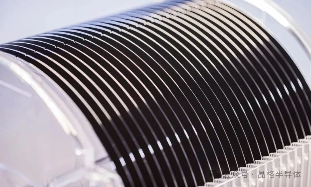
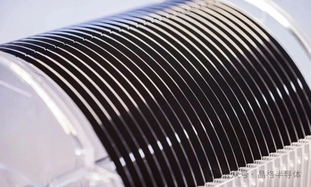
Intuitively, one might think thinner is better since the final chip is thin. In reality, the opposite is true. A 300 mm wafer must endure extensive handling by robotic arms, vacuum chucks, and carriers throughout fabrication. If the wafer is too thin, it becomes more prone to bending and deformation. A 300 mm wafer has a diameter-to-thickness ratio of approximately 387:1, making it a classic thin-plate structure.
Why Does Thickness Matter So Much for Mechanical Stiffness?
The most important principle for understanding 775 μm is this: the bending stiffness of a thin plate is proportional to the cube of its thickness. In a simplified model, the bending stiffness of a circular silicon wafer can be expressed as a function of the elastic modulus, thickness, and Poisson’s ratio. This means a small reduction in thickness can cause a significant drop in stiffness.
For example, if a wafer is thinned from 775 μm to 700 μm, the bending stiffness may drop to approximately 73% of its original value—a thickness reduction of about 10% results in a stiffness reduction of about 27%. This is why wafers cannot simply be made “as thin as possible.”
Why Can’t Wafers Be Made Extremely Thick?
If greater thickness improves stiffness, why not make wafers 1 mm or even 2 mm thick? Several factors prevent this:
- Material cost: Silicon wafers are high-purity semiconductor materials. Greater thickness means more silicon consumption and higher manufacturing costs.
- Process compatibility: Many fabrication processes must account for wafer thickness. Increased thickness can introduce issues with process time, heat conduction, and equipment compatibility.
Engineering design is therefore a balancing act: the wafer must be thick enough to ensure mechanical stability during fabrication, yet not so thick as to waste material and increase manufacturing burden. The 775 μm specification emerged from this industrial environment as one of the common standard specifications for 300 mm wafers.
Summary
A silicon wafer that appears to be simply “300 mm × 775 μm” actually embodies decades of semiconductor manufacturing engineering experience. It is neither a simple geometric dimension nor a result directly calculated from a theoretical formula. The 300 mm represents the wafer platform’s size standard, while 775 μm reflects the comprehensive balance of this platform across mechanics, processes, equipment, and cost.
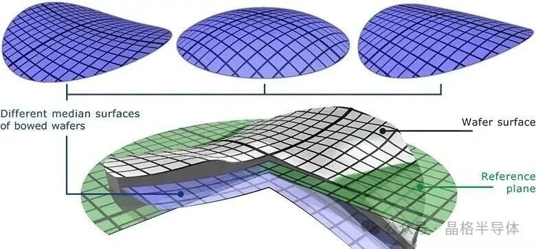
Furthermore, 775 μm is not the endpoint. As wafers enter specific chip fabrication flows, backside thinning, and advanced packaging requirements, they may be further thinned from several hundred micrometers to even thinner states. This naturally leads to important topics such as wafer Bow and Warp, thin-film stress-induced bending, and the high flatness requirements for 300 mm wafers.
기사 출처:Jingge Semiconductor —초대형단결정 실리콘 소재 및 다결정 기둥상 실리콘 소재를 공급합니다. 당사의 제품은 반도체 에칭 공정에 사용되는 실리콘 부품의 가공을 위해 특별히 설계되었으며, 여기에는 직경 최대 650mm의 단결정 실리콘 링, 단결정 실리콘 웨이퍼, 기둥상 결정립 실리콘 링 및 다결정 실리콘 웨이퍼가 포함됩니다.