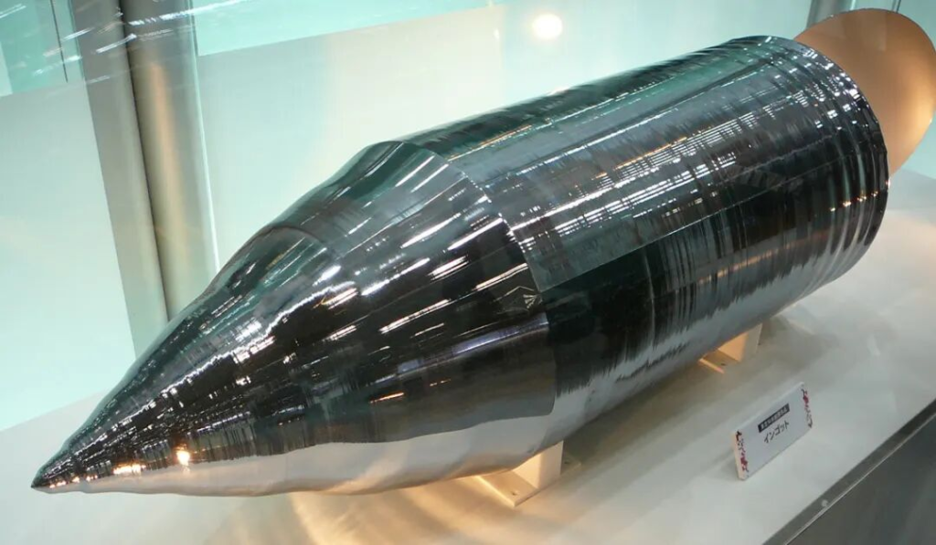
In Czochralski (CZ) silicon, interstitial oxygen atoms themselves are electrically neutral and do not directly change resistivity. What truly affects resistivity are the thermal donors (300–500°C), new donors (550–850°C), and oxygen precipitates (>650°C) formed during subsequent thermal processing – these three oxygen‑derived species alter carrier concentration or introduce recombination centres through different mechanisms, ultimately leading to resistivity changes. Understanding this dynamic process is the prerequisite for precise resistivity control in single‑crystal silicon.
📊 Quick Overview of the Three Mechanisms by Which Oxygen Affects Resistivity
| Mechanism | Temperature Window | Formed Product | Effect on Resistivity | Typical Concentration |
|---|---|---|---|---|
| Thermal Donors | 300–500°C (peak ~450°C) | Electrically active complexes of aggregated oxygen atoms | N‑type ↓ / P‑type ↑ (compensation effect) | ~10¹⁶ cm⁻³ (450°C/100h) |
| New Donors | 550–850°C (>10h) | Complex silicon‑oxygen clusters | Supply electrons, alter carrier concentration | Weaker than thermal donors, spatially localised |
| Oxygen Precipitates | >650°C | Precipitation of supersaturated interstitial oxygen + dislocations/stacking faults | Introduce recombination centres + local stress fields | Related to oxygen supersaturation |
Core logic chain: Interstitial oxygen (electrically neutral) → thermal processing drives migration and aggregation → formation of electrically active derivatives → resistivity change
❓ What Is the Essence of How Oxygen Content Affects Resistivity?
Answer: Many people mistakenly believe that oxygen atoms themselves change the conductivity of silicon, but this is not the case. Interstitial oxygen atoms (Oᵢ) are electrically neutral at room temperature and do not contribute any free carriers.
The real reason lies in the fact that during cooling from the growth temperature (>1400°C) to room temperature, and throughout the various high‑temperature steps in subsequent device manufacturing, the single‑crystal silicon experiences thermal processing across multiple temperature windows. During these thermal treatments, interstitial oxygen atoms migrate, aggregate, and interact with other defects in the lattice, forming electrically active complexes or precipitates – it is these oxygen‑derived species (not oxygen itself) that constitute the true carriers of resistivity change.
❓ How Do Thermal Donors Become the “Resistivity Killer”?
Answer: Thermal donors are the most common and classic mechanism by which oxygen affects resistivity, especially in CZ silicon with relatively high oxygen content.
Formation Conditions
When CZ silicon with high oxygen content undergoes thermal treatment in the 300–500°C range (peak at approximately 450°C), interstitial oxygen atoms aggregate to form a series of electrically active thermal donor complexes. Annealing at 450°C for 100 hours can produce a thermal donor concentration of about 10¹⁶ cm⁻³.
Opposite Effects on N‑type and P‑type Silicon
Since thermal donors supply electrons, they have diametrically opposite effects on the resistivity of N‑type and P‑type silicon:
| Conductivity Type | Effect of Thermal Donors | Resistivity Change |
|---|---|---|
| N‑type silicon | Supplied electrons add to existing electrons | ↓ Decrease (carrier concentration increases) |
| P‑type silicon | Supplied electrons compensate/annihilate existing holes | ↑ Increase (“false high” phenomenon) |
Extreme case: If the thermal donor concentration is high enough, it can even completely convert P‑type silicon into N‑type silicon.
Formation of “Native” Thermal Donors
During the post‑growth cooling process, CZ silicon inevitably passes through the 300–500°C temperature range. Since the crystal head dwells longest near 450°C during cooling and has a higher oxygen content, it generates more thermal donors than the tail – this is a major source of axial resistivity non‑uniformity along the crystal ingot.
How Are Thermal Donors Eliminated in Engineering Practice?
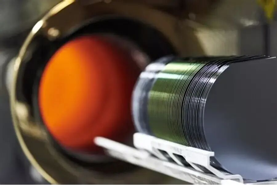
Since thermal donors cause resistivity “distortion,” the standard engineering approach is 650°C annealing for 30–60 minutes, followed by rapid cooling to below 300°C.
Principle: During annealing in the 650–800°C range, oxygen diffusivity increases, and interstitial oxygen begins to nucleate homogeneously and aggregate into oxygen precipitates, reducing the interstitial oxygen concentration and thereby eliminating thermal donors.
Note: If the cooling rate is insufficient, a small fraction of thermal donors may remain. For large‑diameter ingots, rapid cooling can induce thermal stress and cracking, so wafer‑level annealing is typically adopted instead.
❓ How Do New Donors Differ from Thermal Donors?
Answer: New donors are another type of oxygen‑related electrically active defect generated in single‑crystal silicon during prolonged thermal treatment (>10 hours) at 550–850°C.
New Donors vs. Thermal Donors
| Comparison Aspect | Thermal Donors | New Donors |
|---|---|---|
| Formation temperature | 300–500°C (peak 450°C) | 550–850°C (>10h) |
| Formed product | Oxygen‑atom aggregated complexes | Large‑scale silicon‑oxygen clusters |
| Elimination | Can be eliminated by 650°C annealing | More stable; different annealing behaviour |
| Electrical activity | Strong, reversible | Weaker, spatially localised |
The Particularity of New Donors
Studies have shown that in neutron‑transmutation‑doped CZ silicon (NTD CZ Si) , irradiation‑enhanced oxygen diffusion leads to aggregation in disordered regions, forming large‑scale complex silicon‑oxygen clusters – this is the primary mechanism of new donor formation.
An interesting finding from spreading resistance profiling (SRP) studies: for samples with relatively low oxygen content, SRP can detect new donor formation, while four‑point probe resistivity measurements show no observable change – suggesting that the electrical activity of new donors may be weaker than that of thermal donors, or that they are more spatially localised.
❓ How Do Oxygen Precipitates Affect Resistivity?
Answer: When the thermal treatment temperature exceeds 650°C, supersaturated interstitial oxygen further precipitates to form oxygen precipitates, whose impact mechanism is more complex than that of thermal donors.
Pathways of Oxygen Precipitate Influence
Pathway 1: As recombination centres that reduce minority‑carrier lifetime
When the interstitial oxygen concentration exceeds its solid solubility, thermal donors, new donors, and oxygen precipitates form during thermal processing, further generating dislocations, stacking faults, and other defects. These defects act as recombination centres for minority carriers – they do not directly change the majority‑carrier concentration like thermal donors, but they significantly reduce minority‑carrier lifetime and cause micro‑scale resistivity non‑uniformity.
Pathway 2: Introduction of local stress fields
The oxygen precipitates themselves, along with the dislocations and stacking faults they induce, introduce local stress fields in the lattice that affect carrier mobility, thereby causing local resistivity fluctuations.
Distinction from Thermal Donors
Studies indicate that after annealing in the 600–900°C range, significant resistivity drift can be observed – this phenomenon is associated with oxygen precipitates and is independent of the thermal donor effect near 450°C. These are two distinct physical mechanisms.
The “Safe Threshold” for Oxygen Content
Research suggests that when the oxygen content of CZ silicon is below 8×10¹⁷ cm⁻³, the thermal stability of resistivity is relatively good. Below this threshold, even with various thermal treatments, the effects of oxygen precipitates and donor formation remain relatively limited, and resistivity maintains good stability.
❓ Why Is High‑Resistivity Silicon More Sensitive to Oxygen Content?
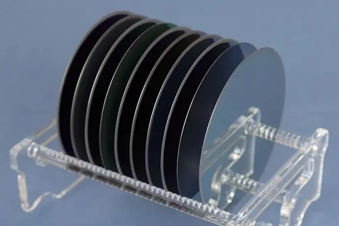
Answer: The degree to which oxygen content affects resistivity depends on the relative relationship between the doping concentration (i.e., the original resistivity) and the concentration of oxygen‑derived species.
| Material Type | Doping Concentration | Typical Resistivity | Thermal Donor Impact | Conclusion |
|---|---|---|---|---|
| Low‑resistivity silicon | ~10¹⁶–10¹⁷ cm⁻³ | 1.68–7.0 Ω·cm | Thermal donors ~10¹⁴ cm⁻³, far below doping concentration | Minor effect |
| High‑resistivity silicon | Low (comparable to or below donor level) | High | Donor concentration can be comparable to or exceed doping level | Dramatic change |
Core rule: The lower the doping concentration (i.e., the higher the resistivity), the more pronounced the oxygen donor effect. This is the fundamental reason why high‑resistivity single‑crystal silicon is more sensitive to oxygen content and thermal history.
❓ How Does Engineering Practice Manage Oxygen‑Induced Resistivity Interference?
Answer: Oxygen plays a dual role in single‑crystal silicon – both beneficial and detrimental – and engineering practice must carefully balance the two.
The Dual Role of Oxygen
| Beneficial Effects | Detrimental Effects |
|---|---|
| ✅ Pins dislocations, improves mechanical strength | ❌ Thermal donors cause resistivity “distortion” |
| ✅ Acts as internal gettering centres to remove metallic impurities | ❌ New donors exacerbate resistivity instability |
| — | ❌ Oxygen precipitates reduce minority‑carrier lifetime and introduce stress fields |
Four Core Control Strategies
Strategy 1: Control oxygen content during crystal growth
Adjust parameters such as crucible rotation rate, crystal rotation rate, argon flow rate, and chamber pressure to control the dissolution and volatilisation of oxygen from the quartz crucible into the melt, thereby controlling oxygen content at the source.
Strategy 2: Eliminate native thermal donors
Apply 650°C annealing (30–60 minutes) to as‑grown ingots or sliced wafers to eliminate thermal donors formed during cooling and restore resistivity to its true value.
Strategy 3: Rapidly cross the “dangerous temperature zone”
During the post‑growth cooling process, cross the 300–500°C range as quickly as possible to minimise thermal donor formation.
Strategy 4: Control oxygen content at the source
Maintain the oxygen content of single‑crystal silicon below 8×10¹⁷ cm⁻³ to fundamentally improve the thermal stability of resistivity.
기사 출처:Jingge Semiconductor —초대형단결정 실리콘 소재 및 다결정 기둥상 실리콘 소재를 공급합니다. 당사의 제품은 반도체 에칭 공정에 사용되는 실리콘 부품의 가공을 위해 특별히 설계되었으며, 여기에는 직경 최대 650mm의 단결정 실리콘 링, 단결정 실리콘 웨이퍼, 기둥상 결정립 실리콘 링 및 다결정 실리콘 웨이퍼가 포함됩니다.