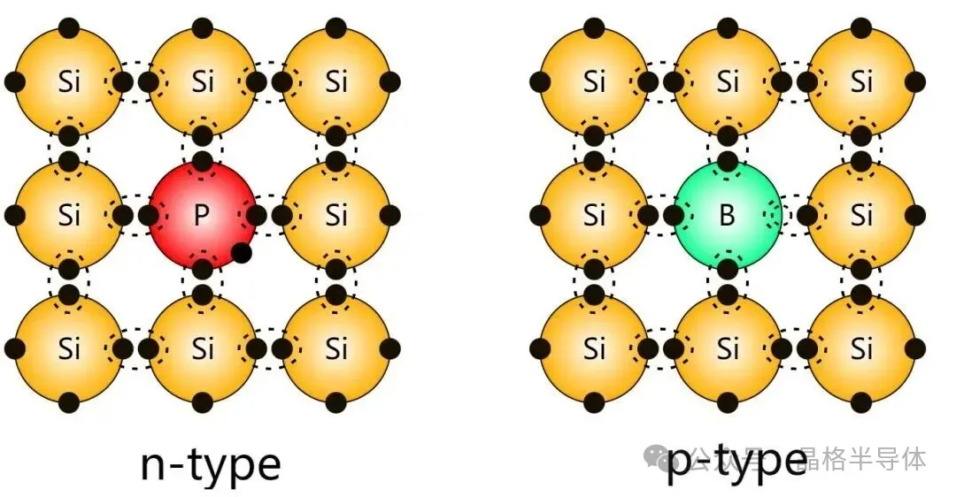
Semiconductor doping can be classified along two independent dimensions: physically as substitutional vs. interstitial doping, and electronically as heterovalent vs. isovalent doping. Substitutional doping (where B, P, As occupy lattice “seats”) is the fundamental mechanism for achieving electrical conductivity control, while heterovalent doping (with 3‑ or 5‑valence impurities) is the core means of altering resistivity and conductivity type. Understanding these four doping types provides the theoretical foundation for selecting and evaluating doping processes.
📊 Quick Overview of the Four Doping Types
| Classification Dimension | Doping Type | Effect on Electrical Performance | Typical Process Means |
|---|---|---|---|
| Physical Position | Substitutional | ✅ Activates conduction (provides carriers) | Thermal diffusion, ion implantation after annealing, in‑situ doping |
| Physical Position | Interstitial | ❌ Usually inactive (requires annealing to eliminate) | Un‑annealed ion implantation; diffusion of certain metals (e.g., Au) |
| Valence Effect | Heterovalent | 🔄 Significantly changes resistivity and conductivity type (N/P) | Ion implantation, thermal diffusion (mainstream for device fabrication) |
| Valence Effect | Isovalent | ➖ Almost no change in resistivity (no carrier contribution) | Crystal growth or epitaxy: in‑situ doping, melt doping |
❓ What Are Substitutional and Interstitial Doping, and What Is Their Fundamental Difference?
Answer: The difference lies in where the impurity atom ends up after entering the silicon lattice.
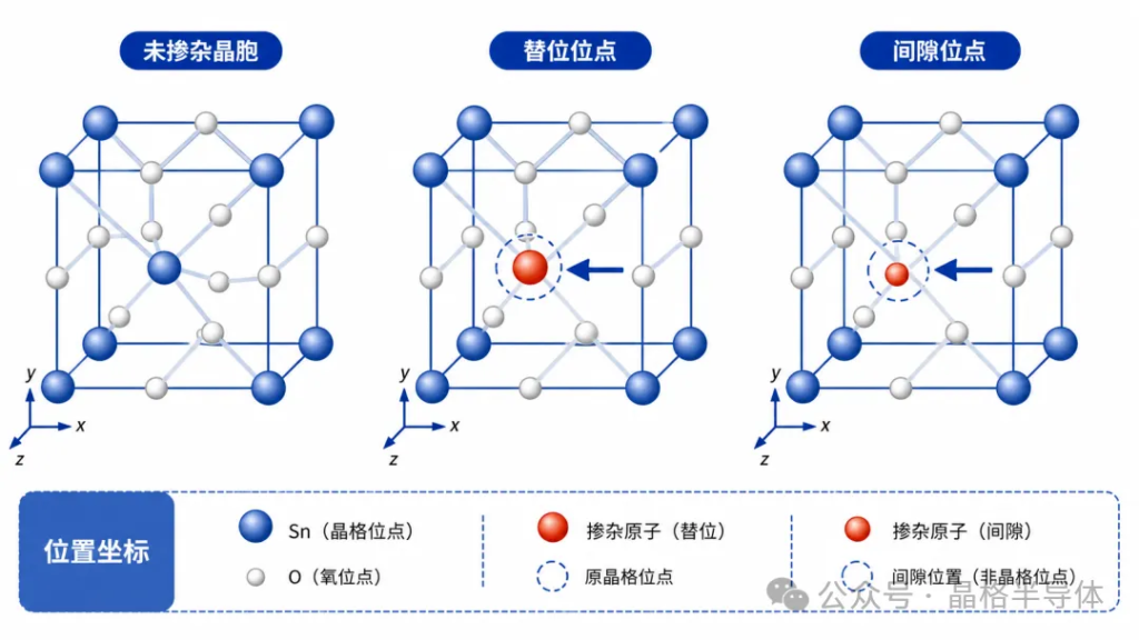
Substitutional Doping — Occupying the “Regular Seat”
- Definition: Impurity atoms replace the original silicon atoms in the lattice, occupying a lattice node position.
- Electrical effect: This is the only doping mode that achieves electrical activation. Only when impurities (such as B, P, As) sit in substitutional positions can they provide free electrons or holes.
- Typical processes: Thermal diffusion, ion implantation (after annealing), in‑situ doping – all these aim to place impurity atoms into the lattice “regular seats.”
- Analogy: Like a regular employee sitting in their assigned workstation, starting to work properly (contributing to conductivity).
Interstitial Doping — Squeezing into the “Aisle”
- Definition: Impurity atoms squeeze into the interstitial spaces between lattice atoms, rather than replacing silicon atoms.
- Electrical effect: Usually does not contribute to conductivity (inactive), and instead disrupts lattice integrity.
- Typical process: Often a side effect – during ion implantation, high‑energy ions damage the lattice, and many impurity atoms get “stuck” in interstitial positions.
- Remediation: Requires high‑temperature annealing to give interstitial atoms enough energy to jump back to substitutional “seats.”
- Exceptions: Some very small atoms (e.g., oxygen, gold) can be deliberately placed interstitially for gettering or minority‑carrier lifetime control.
- Analogy: Like someone squeezed into a crowded office aisle – not only unable to work properly, but also obstructing others.
Key mnemonic: Substitutional = “regular seat” ✅ works; Interstitial = “crowded aisle” ❌ causes trouble.
❓ What Are Heterovalent and Isovalent Doping, and How Do They Differ in Conductivity Effects?
Answer: The difference lies in whether the impurity atom has more, fewer, or the same number of valence electrons compared to silicon.
Heterovalent Doping — Different Valence Electron Count
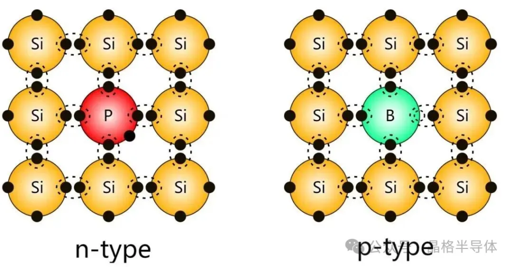
- Definition: Impurity atoms have a different valence from silicon (4) – either 3 or 5.
- Electrical effect: This is the core of semiconductor conductivity control. It significantly changes resistivity and conductivity type (N‑type or P‑type).
- Typical impurities: Boron (3‑valence), Phosphorus (5‑valence), Arsenic (5‑valence).
- Typical processes: Ion implantation, thermal diffusion – the mainstream doping processes for all device manufacturing.
- Core principle:
- 3‑valence impurity → creates holes (P‑type conduction)
- 5‑valence impurity → creates free electrons (N‑type conduction)
Isovalent Doping — Same Valence Electron Count
- Definition: Impurity atoms have the same valence as silicon (4).
- Electrical effect: Generates neither free electrons nor holes; resistivity remains almost unchanged.
- Typical impurities: Germanium (Ge), Carbon (C).
- Typical processes: During crystal growth or epitaxy (in‑situ doping, melt doping).
- Main purposes:
- Adjust lattice stress (e.g., Ge doping to suppress dislocation slip)
- Improve mechanical strength
- Control point defects
- Not intended to change electrical performance
Key mnemonic: Heterovalent = different electron count → big change in conductivity; Isovalent = same electron count → no change in conductivity.
❓ Why Can Substitutional Doping Only Be Achieved Through Specific Processes?
Answer: Because the way impurity atoms enter the lattice depends on process conditions and energy input.
| Process | Entry Mode | Can It Achieve Substitutional Doping? | Reason |
|---|---|---|---|
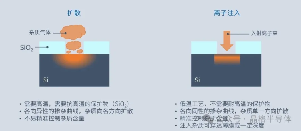
| 열 확산 | Atomic thermal motion at high temperature (>900°C) | ✅ Yes | High temperature provides sufficient energy for atoms to overcome the potential barrier and enter lattice nodes. |
| Ion Implantation (un‑annealed) | Forced injection by high‑energy ions | ❌ No (mostly interstitial) | High‑energy impact disorders the lattice; atoms are “stuck” interstitially and inactive. |
| Ion Implantation (+ annealing) | Post‑implantation high‑temperature repair | ✅ Yes | Annealing gives interstitial atoms enough energy to jump back to substitutional positions. |
| 현장 도핑 | Direct incorporation during epitaxial growth | ✅ Yes | Atoms occupy lattice nodes directly as the epitaxial layer forms. |
Core insight: Substitutional doping requires impurity atoms to have sufficient energy to “squeeze” into lattice nodes and stabilise there. Thermal diffusion and in‑situ doping naturally satisfy this condition; ion implantation relies on subsequent annealing to complete the “interstitial → substitutional” conversion.
❓ What Is the Practical Use of Isovalent Doping in Production?
Answer: Although isovalent doping does not change electrical properties, it plays an irreplaceable role in crystal quality engineering.
Major Application 1: Germanium (Ge) Doping – Dislocation Density Control
- Effect: Ge atoms are similar in size to Si but slightly larger; incorporation relieves lattice thermal stress and reduces dislocation density.
- Typical scenario: Large‑diameter single‑crystal silicon growth (Ge‑doped CZ wafers).
- Outcome: Improved mechanical strength, reduced breakage during processing.
Major Application 2: Carbon (C) Doping – Point Defect Engineering
- Effect: Carbon atoms are smaller than silicon and can occupy substitutional sites, suppressing oxygen precipitation and vacancy aggregation.
- Typical scenario: Epitaxial layer growth.
- Outcome: Improved device leakage characteristics and reliability.
Major Application 3: SiGe Alloys
- Effect: High‑concentration Ge doping (up to 20–30%) forms SiGe alloys for bandgap engineering.
- Typical scenarios: SiGe HBTs (heterojunction bipolar transistors), strain engineering for CMOS channels.
- Outcome: Significantly enhanced carrier mobility, enabling higher frequency and lower power consumption.
Key point: Isovalent doping does not change conductivity type, but it optimises lattice quality – it is the tool of the “materials engineer,” while the “device engineer” relies more on heterovalent doping.
❓ How Can We Summarise the Four Doping Types in a Single Table?
Answer: The table below compares the four doping types across four dimensions:
| Comparison Dimension | Substitutional | Interstitial | Heterovalent | Isovalent |
|---|---|---|---|---|
| Core Question | Where is the atom? | Where is the atom? | How many valence electrons? | How many valence electrons? |
| Effect on Lattice | Regular replacement, structural integrity | Occupies interstices, creates defects | Provides carriers, modifies band structure | Adjusts stress, no carrier contribution |
| Conductivity Change | Substantial | Almost none (inactive) | Substantial | Almost none |
| Typical Impurities | B, P, As, Sb | Un‑annealed B/P/As; interstitial O, Au | B (3‑valence), P/As (5‑valence) | Ge (4‑valence), C (4‑valence) |
| Process Means | Thermal diffusion, annealed ion implantation, in‑situ | Un‑annealed ion implantation | Ion implantation, thermal diffusion | Crystal growth, epitaxy |
| Electrically Active? | ✅ Yes | ❌ No | ✅ Yes (generates carriers) | ❌ No |
❓ What Guidance Does This Provide for Practical Process Selection?
Answer: Understanding these four doping types helps engineers make more accurate decisions in process design and problem diagnosis.
1. Selection Logic in Process Design
| Scenario | Preferred Doping Type | Reason |
|---|---|---|
| Fabricating PN junctions, transistors | Heterovalent (B/P/As) | Need to change conductivity type and generate carriers |
| Improving wafer mechanical strength | Isovalent (Ge doping) | Does not interfere with electrical performance, only improves mechanical properties |
| Ultra‑shallow junctions (advanced logic) | Ion implantation + rapid thermal annealing | Precise depth control; annealing activates substitutional doping |
| Deep junctions (power devices) | Thermal diffusion | High temperature, long time, stable substitutional doping |
2. Diagnostic Framework When Doping Deviates from Expectation
If doping results deviate from expectations, investigate along two dimensions:
- Physical position: Are the impurities actually in substitutional sites? (Check whether annealing conditions were adequate.)
- Valence effect: Does the chosen impurity’s valence match the target conductivity type? (Confirm impurity species selection.)
💎 Full Summary
Semiconductor doping classifications can be understood along two independent dimensions:
| 차원 | Two Types | Core Distinction | One‑Sentence Mnemonic |
|---|---|---|---|
| Physical Position | Substitutional vs. Interstitial | Where the atom sits | Substitutional = “regular seat”; Interstitial = “crowded aisle” |
| Valence Effect | Heterovalent vs. Isovalent | How many valence electrons differ | Heterovalent = “big electrical change”; Isovalent = “stable structure” |
Final conclusion: Substitutional + heterovalent (e.g., B, P, As occupying lattice nodes) is the golden combination for achieving electrical doping – the core of semiconductor device fabrication. Interstitial + isovalent (e.g., un‑annealed ion‑implanted states, or Ge/C doping) serve other purposes – either as intermediate states (to be eliminated by annealing) or quality engineering (to improve crystal properties). Mastering these four concepts provides a systematic theoretical foundation for doping technology.
기사 출처:Jingge Semiconductor —초대형 단결정 실리콘 및 다결정 실리콘 공급 기둥상 결정 구조 소재를 공급하며, 에칭 링, 샤워 헤드, 배기 링, 포커스 링, 실드 링 등을 포함한 실리콘 부품의 OEM 맞춤형 제작 서비스를 제공합니다.