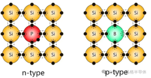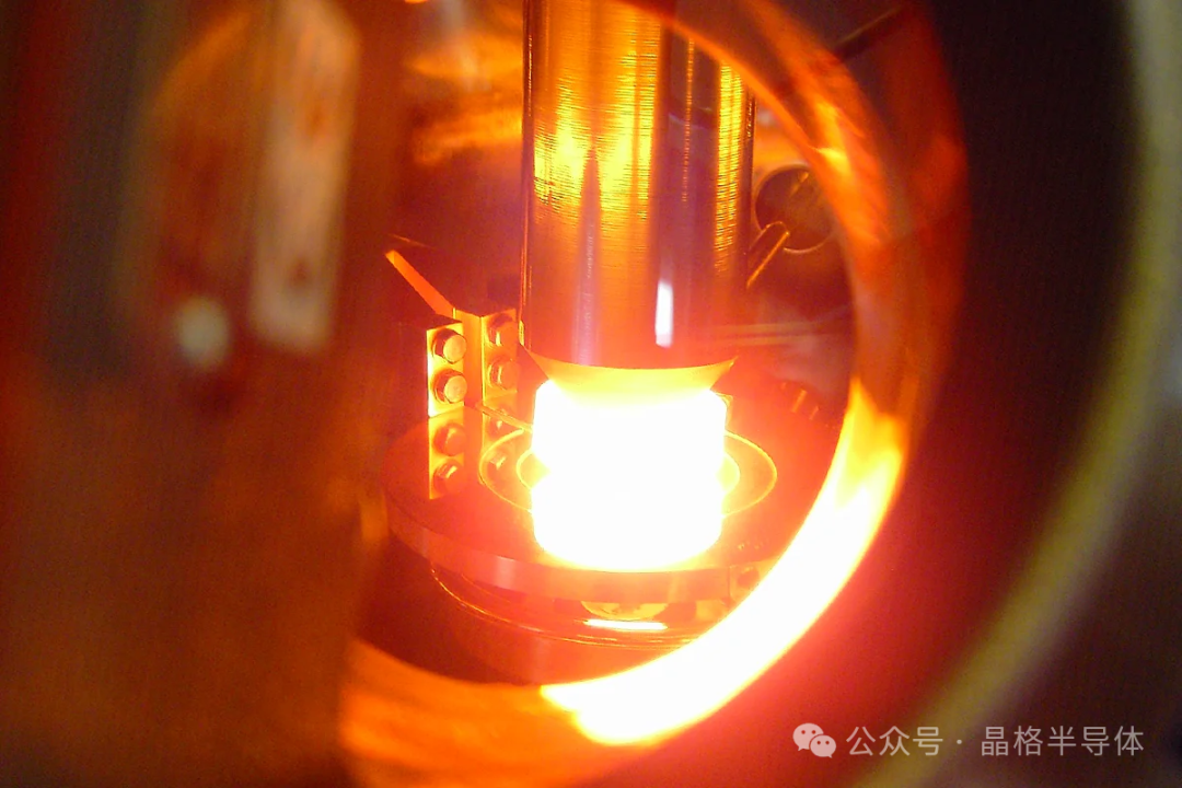
Because the float‑zone (FZ) method does not use a crucible, it cannot be doped by simply adding dopants to the melt as in the Czochralski (CZ) process. Instead, several special doping techniques have been developed for FZ silicon. The main methods are described below.
1. Core Doping (Pre‑doping of the feed rod)
This method introduces the dopant during the preparation of the polysilicon feed rod.
- Principle: When manufacturing the polysilicon rod, a doped silicon core is used, or dopants are incorporated during the deposition process. The feed rod itself thus contains the dopant. During the float‑zone process, the dopant enters the molten zone as the feed rod melts and is finally incorporated into the growing crystal.
- Characteristics: The process is relatively simple, but axial resistivity uniformity is difficult to control because the dopant concentration changes continuously during growth due to the segregation effect.
- Application: Particularly suitable for dopants with a segregation coefficient close to 1, such as boron (B). Boron has a segregation coefficient of about 0.8 in silicon, so its segregation effect is weak, and the axial resistivity distribution can be controlled more easily.
2. Solution Coating Doping
In this method, a solution containing the dopant is coated onto the surface of the feed rod.
- Principle: A solution of the dopant (e.g., boron oxide or phosphorus pentoxide in anhydrous ethanol) is uniformly applied to the surface of the polysilicon rod. During the zone‑melting process, the solvent evaporates and the dopant enters the molten zone, thereby doping the crystal.
- Characteristics: Although seemingly simple, this method has some drawbacks: quantitative control of the dopant is difficult, and the coating may be non‑uniform, leading to poor resistivity uniformity in the final crystal.
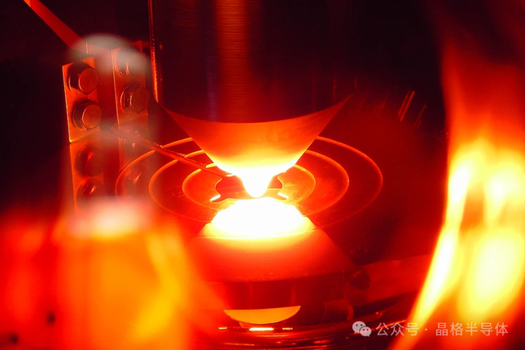
3. Pill / Charge Doping
This method is mainly used for dopants with very low segregation coefficients and low volatility, such as gallium (Ga) and indium (In).
- Principle: A small hole is drilled at a specific position (e.g., near the cone section) of the feed rod, and a high‑purity dopant (e.g., metallic gallium or indium) is placed into the hole. Because these dopants have extremely low segregation coefficients (e.g., gallium ~0.008), their concentration in the molten zone hardly decreases during growth, allowing crystals with very uniform axial resistivity to be grown.
- Application: Gallium‑ or indium‑doped FZ silicon is mainly used in infrared detectors and other special applications.
4. Gas‑Phase Doping (GD)
This is currently the most commonly used and most flexible doping method.
- Principle: During crystal growth, gases containing the dopant elements (e.g., phosphine (PH₃) for n‑type doping, diborane (B₂H₆) for p‑type doping) are introduced directly onto the surface of the silicon melt through a special device (such as a hollow doping coil). The doping gases decompose at high temperature, and the dopant atoms enter the molten zone, achieving real‑time doping of the crystal.
- Characteristics:
- High flexibility: The doping gas flow can be turned on, off, or adjusted at any time during growth, allowing precise resistivity control.
- Good resistivity controllability: By precisely controlling the gas flow rate and other parameters, crystals with excellent axial resistivity uniformity can be obtained.
- Short production cycle and relatively low cost.
- Challenges: The equipment (especially the doping coil) and process control (gas flow, temperature, etc.) require high precision.
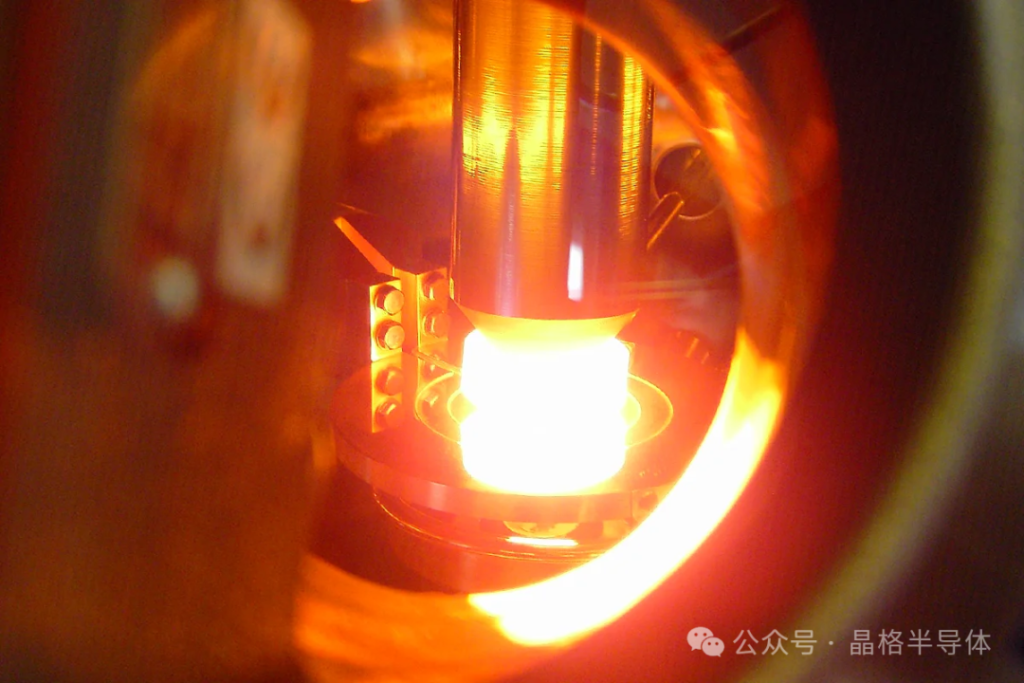
5. Neutron Transmutation Doping (NTD)
This is a very special doping method, mainly used to produce high‑uniformity n‑type FZ silicon.
- Principle: A high‑purity FZ silicon ingot is irradiated with thermal neutrons in a nuclear reactor. About 3.1% of natural silicon atoms are the isotope ³⁰Si. When a ³⁰Si atom captures a thermal neutron, it becomes unstable ³¹Si, which then decays into stable ³¹P (phosphorus) atoms. Phosphorus is an n‑type dopant, so doping is achieved.
- Characteristics:
- Extremely high doping uniformity: Because neutrons have strong penetrating power, the nuclear reaction occurs uniformly throughout the crystal volume, resulting in excellent radial and axial resistivity uniformity. It has been reported that for 80‑mm‑diameter wafers, the doping uniformity can be better than 1%.
- High precision: The final phosphorus concentration (and thus resistivity) can be precisely controlled by adjusting the total neutron fluence.
- Limitations:
- Only for n‑type doping: It only converts silicon into phosphorus.
- Requires a nuclear reactor: The equipment barrier is extremely high and the cost is expensive.
- Produces radioactivity: The irradiated ingot is radioactive (mainly from ³²P, half‑life ~14.3 days) and must be stored for some time until the radioactivity decays to safe levels before further processing.
- Causes lattice damage: The nuclear reaction creates lattice defects, which must be annealed at about 800°C to restore the electrical properties of the material.
Summary
In summary, doping techniques for FZ silicon are chosen according to the required material properties:
- For n‑type doping with ultimate uniformity: Neutron Transmutation Doping (NTD) is the first choice. Although complex and expensive, its unmatched uniformity is essential for high‑voltage power devices.
- For flexible, efficient n‑ or p‑type doping: Gas‑Phase Doping (GD) is the mainstream method, widely adopted for its flexibility and relatively lower cost.
- For specific elements (e.g., boron, gallium): Core doping or pill/charge doping play important roles depending on the specific application.
기사 출처:Jingge Semiconductor —초대형단결정 실리콘 소재 및 다결정 기둥상 실리콘 소재를 공급합니다. 당사의 제품은 반도체 에칭 공정에 사용되는 실리콘 부품의 가공을 위해 특별히 설계되었으며, 여기에는 직경 최대 650mm의 단결정 실리콘 링, 단결정 실리콘 웨이퍼, 기둥상 결정립 실리콘 링 및 다결정 실리콘 웨이퍼가 포함됩니다.