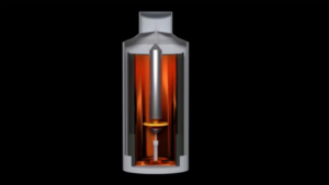
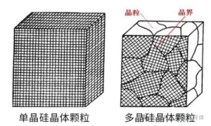
One‑sentence conclusion: Grain boundaries in columnar‑grained silicon ingots originate primarily from simultaneous multi‑point nucleation at the bottom, competitive growth and incomplete elimination of misoriented grains, and thermal stress combined with twinning during cooling. The interplay of these factors creates the dense grain‑boundary network visible in multicrystalline silicon ingots.
For professionals in photovoltaics and semiconductor manufacturing, understanding the formation mechanism of grain boundaries is essential for optimizing casting processes and improving silicon wafer quality.
What Is a Grain Boundary, and Why Can We See a “Network Texture” on a Multicrystalline Silicon Ingot?
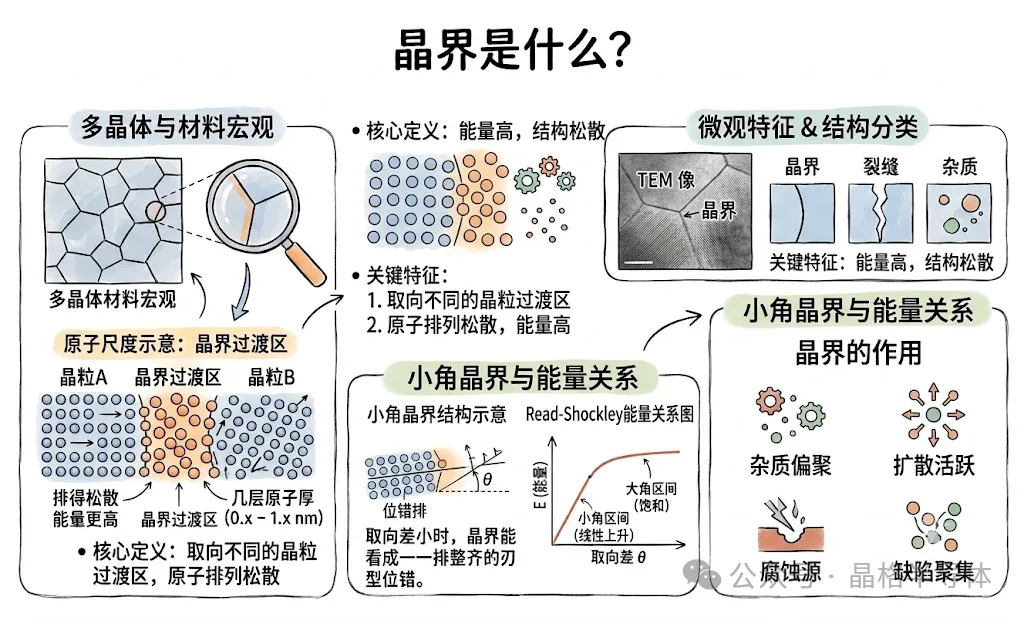
Answer: A grain boundary is the interface where two grains with different crystallographic orientations meet.
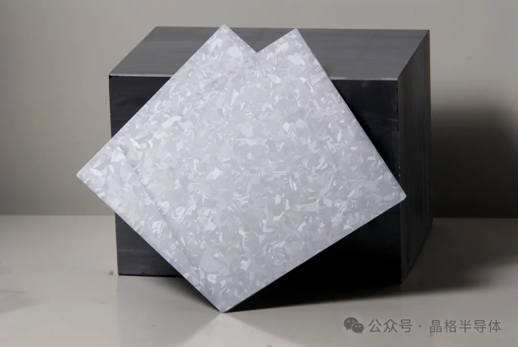
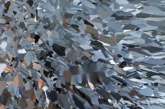
When a multicrystalline silicon ingot is cut open, the naked eye can see a bright‑and‑dark interlaced network pattern – that is the grain boundaries outlining the “grain map”. Because most grains are elongated vertically, resembling columns, this type of ingot is called a columnar‑grained silicon ingot.
Reason 1: Why Are So Many Grain Boundaries Generated at the Very Beginning?
Answer: Because the crucible bottom provides countless nucleation sites where the silicon melt crystallises simultaneously and randomly.
In the directional solidification process, molten silicon first contacts the bottom and side walls of the quartz crucible. The inner wall of the crucible is rough and coated with a silicon nitride (Si₃N₄) layer; these features naturally act as nucleation sites.
When the melt temperature drops below its melting point (supercooling), these sites trigger crystallisation simultaneously. As each nucleation site operates independently, the newly formed grains have random atomic orientations.
Key point: Tens of thousands of grains “spring up” almost at the same time, with chaotic orientations. As soon as they meet each other during early growth, they form a dense network of initial grain boundaries. This step is the root cause of the high boundary density.
Reason 2: Do Grain Boundaries Disappear During Growth?
Answer: No, they do not disappear completely; instead, longitudinal grain boundaries that run through the ingot are formed.
As solidification proceeds from bottom to top, a natural “competitive growth” effect occurs:
- Favourably oriented grains: Grains whose growth direction (usually <100>) is roughly parallel to the heat‑flow direction grow faster and gradually “consume” the surrounding space.
- Unfavourably oriented grains: Grains whose growth direction deviates from the heat flow grow more slowly and are gradually squeezed out by neighbouring “dominant grains”.
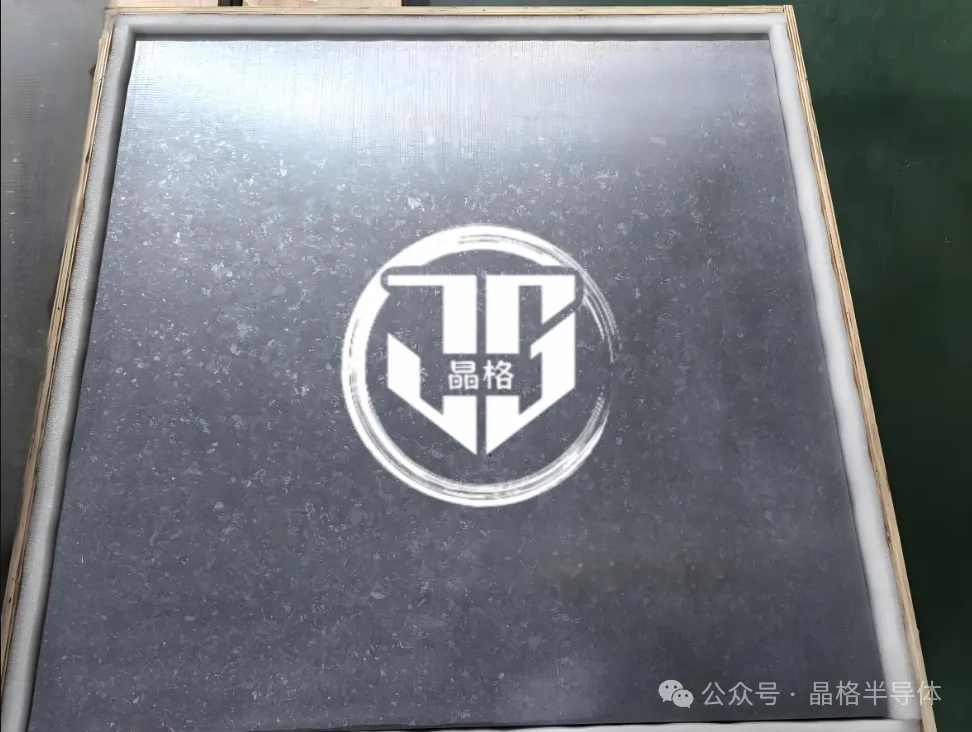
Key point: This process coarsens the grains, but it cannot eliminate all misoriented grains. Eventually, many columnar grains extend from the bottom all the way to the top, and the boundaries between them are longitudinal grain boundaries.
Reason 3: Does the Cooling Process Generate Additional Grain Boundaries?
Answer: Yes. Thermal stress and twinning during cooling add a significant number of extra grain boundaries.
After growth at temperatures above 1400°C, the ingot slowly cools to room temperature. During this stage:
- Thermal stress leads to dislocations and low‑angle grain boundariesNon‑uniform temperature distribution creates enormous thermal stress. Under stress, atomic planes slip, generating a large number of dislocations. The accumulation and arrangement of dislocations produce low‑angle grain boundaries (subgrain boundaries), further increasing the boundary count.
- Twinning – a special type of grain boundarySilicon has a diamond cubic structure with regular atomic arrangement. During growth, twins easily form – that is, atomic layers become mirror‑symmetrical. Twinning is essentially a high‑angle grain boundary, which significantly raises the complexity and density of grain boundaries.
Key point: The superposition of thermal stress and twinning makes the final grain‑boundary density far higher than that produced merely by nucleation and growth.
Summary of the Entire Grain‑Boundary Formation Process
| Stage | Dominant Factor | Grain‑Boundary Type Produced | Impact Level |
|---|---|---|---|
| Nucleation | Multi‑point nucleation on crucible surface | Initial high‑angle boundaries | Numerous; lays the foundation |
| Growth | Competitive growth, survival of the fittest | Longitudinal through‑boundaries | Grains coarsen, boundaries remain |
| Cooling | Thermal stress + twinning | Low‑angle boundaries + twin boundaries | Count multiplies, complexity increases |
Conclusion: Grain boundaries in columnar‑grained silicon ingots are the result of “nucleation sets the baseline, growth determines the distribution, and thermal stress together with twinning finalises the density”.
Article source: Jingge Semiconductor — Supplies ultra‑large monocrystalline Si, poly‑Si columnar‑grained materials, and offers OEM custom fabrication of Si parts, including etch rings, shower heads, exhaust rings, focus rings, and shield rings.