⚡ One‑Sentence Core Conclusion
The silicon focus ring is a critical component surrounding the wafer edge in plasma etching equipment. Through four major functions – plasma physical confinement, electrical compensation and electric field regulation, thermal management, and protection of the electrostatic chuck (ESC) and chamber – it reconstructs the plasma environment at the wafer edge to match the center as closely as possible, thereby solving the edge effect that causes yield loss.
📊 Quick Overview of the Four Major Functions of the Focus Ring
| Function | Core Mechanism | Problem Solved |
|---|---|---|
| Plasma Physical Confinement | Physical barrier limits radial diffusion + shapes sheath boundary + suppresses edge glow discharge | Edge plasma density gradient, ion incidence angle deviation |
| Electrical Compensation & Electric Field Regulation | Capacitive coupling extends potential + reshapes electric field lines + maintains sheath continuity | Edge electric field distortion, lateral etching |
| Thermal Management | Thermal mass buffering + optimized heat conduction path + plasma heating distribution adjustment | Edge temperature non‑uniformity, etch rate variation |
| Protection of ESC & Chamber | Acts as a “sacrificial layer” to absorb plasma bombardment and corrosion | Physical sputtering and chemical corrosion of ESC edge and chamber wall |
❓ What Is the “Edge Effect” in Plasma Etching?
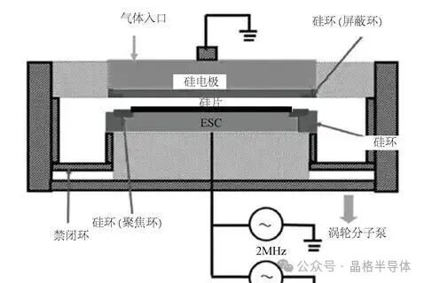
Answer: In plasma etching equipment, the wafer is placed on an electrostatic chuck (ESC), and process gases in the chamber are ionized under RF electric fields to form plasma. Active ions in the plasma bombard the wafer surface vertically under bias voltage, enabling anisotropic etching.
However, the wafer edge and center face completely different physical environments, leading to three core problems:
| Problem | Physical Mechanism | Consequence |
|---|---|---|
| Electric field distortion | The wafer edge is the interface between conductor/semiconductor and surrounding space; electric field lines diverge outward | Ion bombardment angle deviates from vertical, causing lateral etching |
| Plasma density gradient | The sheath morphology at the edge differs from the center; sheath thickness is non‑uniform | Gradient in ion flux and energy distribution |
| Temperature non‑uniformity | Differences in radiation and conduction between edge, ESC edge, and chamber wall | Non‑uniform temperature distribution, affecting etch rate |
Result: The etch rate, etch profile, and selectivity at the wafer edge differ significantly from the center, leading to reduced overall wafer yield. In advanced nodes, this non‑uniformity can cause chips within several millimeters or even tens of millimeters from the edge to be scrapped entirely.
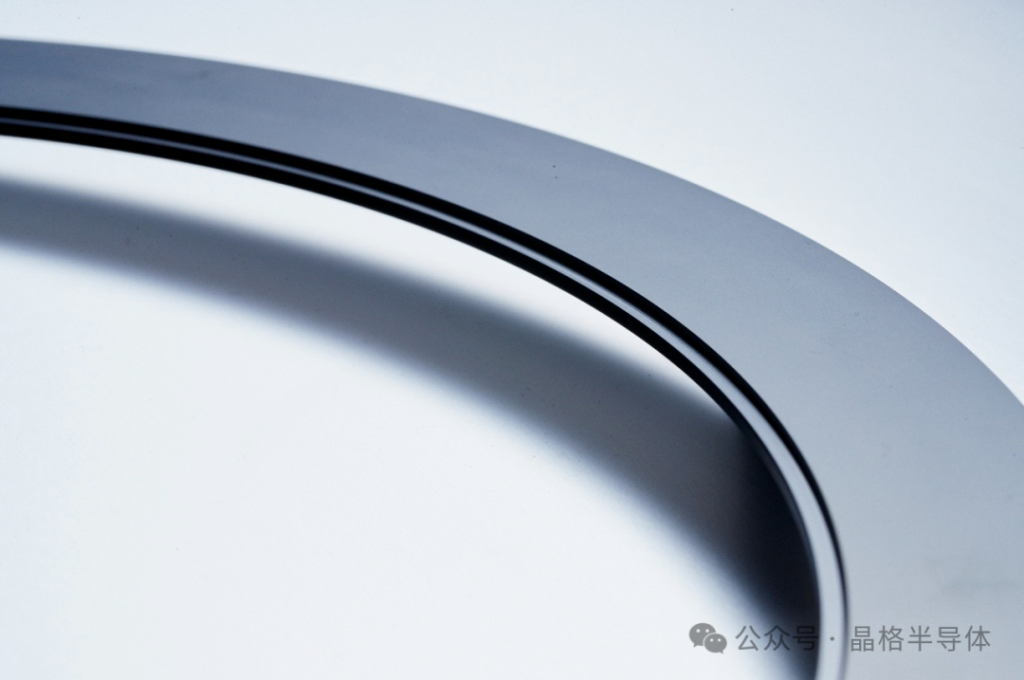
The focus ring is the core component designed to solve this problem. It surrounds the wafer and ESC edge, reconstructing the plasma environment at the wafer edge through physical confinement and electrical compensation to match the center as closely as possible.
❓ Function 1: How Does the Focus Ring Achieve Plasma Physical Confinement?
Answer: The focus ring confines edge plasma through three physical mechanisms.
Mechanism 1: Limiting Radial Plasma Diffusion
Ions and electrons in the plasma naturally diffuse outward driven by concentration gradients. Without physical barriers, the plasma density at the wafer edge decreases due to outward diffusion, forming a density gradient.
The focus ring is an annular structure of a certain height, with an inner diameter slightly larger than the wafer diameter (typically 0.5–2 mm larger), surrounding the wafer edge. This annular wall forms a physical barrier that effectively limits radial outward diffusion of plasma, maintaining the plasma density above the wafer edge close to that of the center.
Mechanism 2: Shaping the Sheath Boundary
A dark region exists between the plasma and the wafer surface, called the ion sheath. Within the sheath, electron density is extremely low, and ions are accelerated to bombard the wafer surface. The sheath boundary at the wafer edge bends outward due to lack of confinement, causing the ion incidence angle to deviate from vertical.
The presence of the focus ring changes the sheath boundary conditions at the edge. Its top surface is at a similar height to the wafer surface, making the sheath boundary flatter at the wafer edge and the ion incidence angle closer to vertical. Studies show that the height of the focus ring and the relative position of its top surface to the wafer surface are key geometric parameters determining edge etch uniformity.
Mechanism 3: Suppressing Edge Glow Discharge
At sharp edges of the wafer, electric field strength concentrates due to the tip effect, potentially triggering local glow discharge and generating non‑uniform plasma. The annular structure of the focus ring smooths the electric field distribution at the edge, suppressing this local discharge phenomenon.
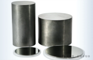
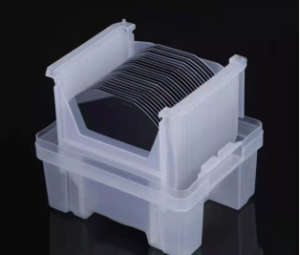
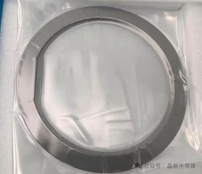
Jingge Semiconductor provides ultra‑large‑size single‑crystal silicon materials and polycrystalline columnar‑grained silicon materials. Products are suitable for processing silicon components used in semiconductor etching, including single‑crystal silicon rings, single‑crystal silicon wafers, columnar‑grained silicon rings, and polycrystalline silicon wafers, with diameters up to 650 mm.
❓ Function 2: How Does the Focus Ring Achieve Electrical Compensation and Electric Field Regulation?
Answer: The focus ring corrects electric field distortion at the wafer edge through electrical compensation mechanisms.
Principle 1: The “Extension” Effect of the Edge Electric Field
The wafer and ESC are typically under RF bias, while the chamber wall is usually grounded. This creates an electric field gradient from the wafer surface to the chamber wall at the wafer edge. In the center region, electric field lines are essentially perpendicular to the wafer surface; but at the edge, electric field lines bend toward the chamber wall, causing ion bombardment direction to deviate from vertical and producing lateral etching.
Principle 2: The Focus Ring as an “Electric Field Extender”
When the focus ring is made of conductive or semi‑conductive materials (such as silicon or silicon carbide), it compensates the edge electric field through the following mechanisms:
| Compensation Mechanism | Principle |
|---|---|
| Capacitive coupling effect | Capacitive coupling exists between the focus ring and the ESC edge. Under RF bias, a potential similar to the wafer surface is induced on the focus ring surface, “extending” the equipotential surface of the wafer to the focus ring |
| Electric field line reshaping | Since the focus ring potential is similar to the wafer, electric field lines originally bending from the wafer edge to the chamber wall now extend vertically upward from the focus ring surface, then bend toward the wall further away. This makes the electric field distribution above the wafer edge closer to the center |
| Sheath continuity | The top surface of the focus ring and the wafer surface together form a continuous sheath boundary. When the potential and geometric parameters match, the sheath thickness and electric field distribution at the edge become consistent with the center |
Principle 3: The Critical Role of Material Conductivity
The conductivity of the focus ring material directly affects its electrical compensation effect:
| Conductivity | Representative Material | Effect |
|---|---|---|
| Too high | Metals | Surface potential too uniform, may differ from wafer surface potential, actually worsening edge electric field distortion |
| Too low | Quartz | Surface cannot effectively induce potential, failing to extend the electric field; edge effect not compensated |
| Moderate (semi‑conductive) | Silicon, silicon carbide | Ideal range: can both induce RF potential and form good electrical matching with the wafer surface |
Silicon has become the mainstream choice for focus rings precisely because its electrical properties are completely consistent with the wafer itself – it is essentially an “extended wafer.”
❓ Function 3: How Does the Focus Ring Achieve Thermal Management and Temperature Uniformity?
Answer: The focus ring improves temperature uniformity at the wafer edge through thermal compensation mechanisms.
Non‑uniformity of the Edge Thermal Environment
The thermal environment at the wafer edge differs significantly from the center:
| Thermal Factor | Edge vs. Center Difference |
|---|---|
| Radiation heat loss | Edge can radiate heat directly to the chamber wall; center is shielded by surrounding wafer |
| Conduction heat loss | Heating/cooling efficiency at the ESC edge is typically lower than at the center |
| Plasma heating | Differences in edge plasma density lead to non‑uniform heating power |
These factors together cause the wafer edge temperature to be lower or higher, affecting etch rate and selectivity.
Thermal Compensation Mechanisms of the Focus Ring
| Compensation Mechanism | Principle |
|---|---|
| Thermal mass buffering | The focus ring has a certain thermal mass, buffering temperature fluctuations at the edge and making wafer edge temperature more stable |
| Heat conduction path | Heat is conducted between the focus ring and ESC through contact. Its thermal conductivity affects edge heat dissipation efficiency. Silicon carbide has an extremely high thermal conductivity (~120 W/m·K, three times that of silicon), enabling more effective heat transfer from the wafer edge to the ESC |
| Plasma heating distribution | The geometry and material of the focus ring affect the edge plasma distribution, thereby influencing the plasma heating power at the wafer edge |
❓ Function 4: How Does the Focus Ring Protect the ESC and Chamber?
Answer: The focus ring acts as a “sacrificial part,” protecting the most expensive and critical components of the etching equipment.
Protection 1: Protecting the ESC Edge
The electrostatic chuck is one of the most expensive components in etching equipment. If its edge region is directly exposed to plasma, it suffers severe physical sputtering and chemical corrosion. The focus ring covers the ESC edge, acting as a “sacrificial layer” that diverts plasma bombardment and corrosive gas attack to itself, thereby protecting the ESC.
Protection 2: Protecting the Chamber Wall
The focus ring also helps protect the chamber wall to some extent. It limits plasma diffusion toward the wall, reducing ion bombardment and chemical corrosion on the wall.
Protection 3: A Replaceable “Sacrificial Part”
For this reason, the focus ring is designed as a replaceable consumable. When it has been eroded by prolonged plasma bombardment to a certain extent, it can simply be replaced with a new one, without replacing the expensive ESC or chamber.
❓ Why Has Focus Ring Material Evolved from Quartz to Silicon, Silicon Carbide, and Boron Carbide?
Answer: The evolution of focus ring materials reflects the core contradiction between electrical matching and long lifetime.
| Material | Electrical Matching | Corrosion Resistance | Thermal Conductivity | Evolution Logic |
|---|---|---|---|---|
| Quartz | ❌ Insulating, cannot provide electrical compensation | Moderate | Low | Gradually phased out |
| Silicon | ✅ Completely matches wafer | Insufficient | Moderate | Current mainstream |
| Silicon carbide | ✅ Good matching | Significantly improved | Extremely high (~120 W/m·K) | Current upgrade direction |
| Boron carbide | Good matching | Ultimate lifetime | High | Future direction |
Core contradiction: Electrical matching requires materials with properties similar to the wafer, while long lifetime requires materials with corrosion resistance beyond that of the wafer. Progress in materials science is precisely the continuous search for the optimal solution within this contradiction.
Article source: Jingge Semiconductor — Supplies ultra‑large‑size single‑crystal silicon materials and polycrystalline columnar‑grained silicon materials. Our products are specifically designed for the processing of silicon components used in semiconductor etching applications, including single‑crystal silicon rings, single‑crystal silicon wafers, columnar‑grained silicon rings, and polycrystalline silicon wafers, with diameters up to 650 mm.