A particle that appears to be only tens or hundreds of nanometers in size can directly become a “chip defect source” during wafer fabrication. This is the core reason why semiconductor silicon wafers must strictly control surface particles.
1. Particles Can Obscure or Damage Lithography Patterns
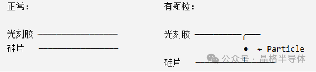
During photolithography, the wafer surface is first coated with photoresist, then exposed and developed. If particles exist on the silicon wafer surface:
- Particles cause localized photoresist thickness variation, exposure defocus, pattern deformation, or even line breakage.
- At advanced nodes, lithography feature sizes continue to shrink, so the allowable particle size also becomes smaller and smaller.
2. Particles Can Cause “Killer Defects”
Suppose a 100 nm particle lands on a wafer. If it happens to be located at:
- Gate region
- Metal interconnect
- Contact/Via
- SRAM cell
- FinFET / GAA nanostructure
Then it may cause: Particle → Pattern defect → Circuit open/short → Die failure
Therefore, fabs care about far more than “How many particles are there?” They care about: “Where is the particle, how large is it, and what material is it?”
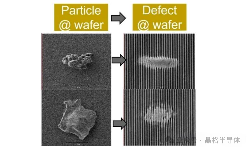
3. Particles Affect Thin Film Deposition and Etching
For example, when depositing a thin film: beneath the particle, localized shadowing, voids, thickness anomalies, or stress concentration may form. During subsequent etching, CMP, ion implantation, and other processes, this location may further amplify into a defect. Therefore, particles often have a characteristic: What starts as a very small particle can become a large electrical defect after dozens of process steps.
Jingge Semiconductor — Supplies ultra-large-size single-crystal silicon materials and polycrystalline columnar-grained silicon materials. Products are suitable for processing silicon components used in semiconductor etching, including single-crystal silicon rings, single-crystal silicon wafers, columnar-grained silicon rings, and polycrystalline silicon wafers, with diameters up to 650 mm. For details.
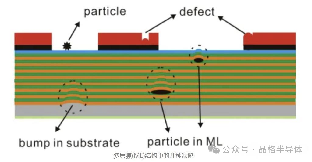
4. Particles Can Also Cause Scratches During CMP
This is especially important for wafer manufacturing itself. For example, in CMP (Chemical Mechanical Polishing): if particles are trapped between the polishing pad and the wafer, they may produce:
- Scratch
- Pit
- Haze
- Localized polishing anomalies
And scratches themselves can generate more particles, creating a vicious cycle of contamination.
5. Particle Count Standards
For 300 mm (12-inch) silicon wafers, SEMI standards have explicit control requirements for surface particles:
| Process Node | Critical Particle Size | Allowable Particle Count (per wafer) |
|---|---|---|
| 90 nm | >45 nm | ≤ 50 |
| 28 nm | >20 nm | ≤ 30 |
| 14 nm | >15 nm | ≤ 20 |
| 7 nm | >10 nm | ≤ 10 |
| 3 nm | >7 nm | ≤ 5 |
Key understanding: It is not simply “the fewer particles, the better.” Rather, every particle larger than the critical size may cause a killer defect. At the 3 nm node, the number of killer particles on a single 300 mm wafer must be controlled to single digits.
Welcome to join my knowledge community — a relatively comprehensive learning platform for the domestic silicon-based industry chain, containing thousands of industry documents. The content is much richer than the articles and is suitable for rapidly improving personal capabilities.