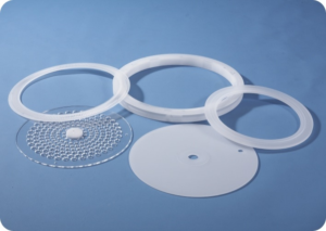
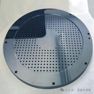
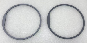
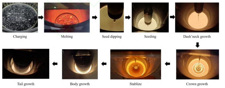
In Czochralski (CZ) monocrystalline silicon growth, the Dash necking process reduces the crystal diameter to 2–4 mm during the seeding stage, allowing dislocations introduced by thermal shock in the seed crystal to slip to the surface and annihilate, thereby producing dislocation‑free monocrystalline silicon. However, a “dislocation‑free” state is not permanent. During the middle and later stages of constant‑diameter growth, the shouldering phase, and even the tail‑end detachment process, multiple physical mechanisms can cause dislocations to re‑nucleate and multiply, ultimately rendering the entire silicon ingot unusable.
The following sections systematically elaborate on the physical origins of dislocations in the later stages of growth, covering thermal stress, solid‑liquid interface, constitutional supercooling, process disturbances, and impurities.
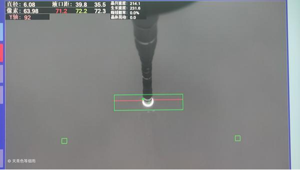
I. Accumulation of Thermal Stress and Dislocation Multiplication
This is the primary cause of dislocations in the later stages of growth. As the silicon ingot diameter increases (to 300 mm or even 450 mm) and length extends, the radial and axial temperature gradients within the crystal continue to rise. The temperature difference between the central region and the edge of the monocrystalline silicon increases significantly; heat in the center cannot be rapidly conducted away, leading to continuous accumulation of thermal stress. When thermal stress exceeds the critical resolved shear stress (CRSS) of silicon at high temperatures, slip systems on {111} planes along 〈110〉 directions are activated, generating slip dislocations.
More critically, dislocations exhibit an exponential multiplication mechanism. According to the Alexander‑Haasen model, once a small number of dislocations already exist in the crystal (even at extremely low density), under sustained high‑temperature thermal stress, the dislocation density will multiply exponentially. This means that even if only a very few dislocation “seeds” are generated in the later stages of growth, they can “infect” the entire silicon ingot to an unusable dislocation density level within a short time. This problem is particularly severe for large‑diameter silicon ingots. Studies have shown that when silicon crystal diameter reaches 300 mm, thermal‑stress‑induced dislocations have become a serious challenge for both FZ and CZ methods.
II. Instability of the Solid‑Liquid Interface Shape
The shape of the solid‑liquid interface has a decisive influence on dislocation generation. In the later stages of constant‑diameter growth, as the melt level in the crucible drops and the melt height decreases, the exposed crucible wall height continuously increases, causing persistent changes in melt convection patterns and heat transfer conditions. These changes directly alter the solid‑liquid interface shape.
Studies have shown that changes in solid‑liquid interface shape lead to non‑uniform distribution of thermal stress, and regions of thermal stress concentration become preferred sites for dislocation nucleation. Specifically:
- A solid‑liquid interface convex toward the melt induces large edge shear stresses, generating edge dislocations;
- A concave solid‑liquid interface is even more prone to dislocation generation and slip;
- A planar interface can effectively suppress dislocation formation.
In heavily doped n‑type monocrystalline silicon, the evolution of the solid‑liquid interface and the formation of {111} edge facets may also promote the generation of supercooled regions, thereby interrupting top‑cone growth and triggering dislocations.
III. Constitutional Supercooling
Constitutional supercooling is another important mechanism for dislocation generation in the later stages of growth. During the constant‑diameter, shouldering, and shoulder‑termination phases, severe constitutional supercooling may occur in local regions of the solid‑liquid interface. When constitutional supercooling occurs, the actual temperature of the melt ahead of the solid‑liquid interface falls below its liquidus temperature, causing interface instability and forming cellular or dendritic interfaces. This unstable interface captures inclusions in the melt and induces microscopic local rotation of crystal orientation, ultimately forming dislocations.
The severity of constitutional supercooling is directly related to crystal growth rate, temperature gradient, and impurity concentration. In the later stages of growth, as melt volume decreases and impurities continuously enrich in the remaining melt, the risk of constitutional supercooling further increases.
IV. Diameter Fluctuations and Process Disturbances
Maintaining stable crystal diameter during the constant‑diameter phase is critical. Severe diameter fluctuations can cause dislocation defects in crystal growth.
Sources of diameter fluctuations include:
- Pull rate fluctuations: Pull rate directly affects the interface shape between crystal and melt, as well as crystal stress distribution. Abnormalities in pull rate and crucible rotation speed can both cause diameter non‑uniformities and dislocations in the silicon ingot.
- Thermal field fluctuations: Thermal convection in the melt (especially strong convection in large‑diameter crucibles) causes temperature fluctuations and local remelting of the crystal, which in turn triggers diameter fluctuations.
- Mechanical drive instability: Instability in the furnace body and mechanical drive systems is also an important factor contributing to dislocations.
In large‑diameter monocrystalline growth, the difficulty of diameter control rises exponentially, and any minor process disturbance can be amplified into a stress concentration sufficient to generate dislocations.
V. Inducing Effects of Impurities and Precipitates
The influence of impurities on dislocations in the later stages of growth has a dual nature:
Beneficial aspects: Impurities such as boron, germanium, nitrogen, phosphorus, arsenic, and oxygen all exert varying degrees of suppression on dislocations, mainly due to the pinning effect of impurity atoms on dislocations. Oxygen atoms can strengthen the silicon lattice by pinning dislocations and delaying slip.
Detrimental aspects: When impurity concentration is too high or unevenly distributed, impurities can instead become sources of dislocation nucleation. For example:
- Excessive impurities in the melt are a major factor causing edge breakage and drop‑off;
- During cooling, supersaturated interstitial atoms precipitate within the silicon wafer, releasing a large number of self‑interstitial silicon atoms that aggregate in certain regions to form dislocations;
- Oxide precipitates may induce secondary defects such as dislocations and stacking faults.
In the later stages of growth, due to the segregation effect, impurities continuously enrich in the remaining melt, with concentrations steadily rising, and the risk of impurity‑induced dislocations increases accordingly.
VI. Thermal Shock During Tail‑End and Detachment Stages
After constant‑diameter growth is completed, if the crystal is immediately separated from the melt, the enormous thermal stress generates a large number of dislocations and slip lines in the crystal tail, which extend upward along the crystal for a length approximately equal to one crystal diameter.
Therefore, tail growth is indispensable: the crystal diameter must be slowly reduced until it tapers to a point before separating from the melt surface. The tail‑growth process minimizes thermal stress effects by reducing the effective area subjected to thermal stress at the crystal tail, thereby maximally preventing dislocation generation. However, tail growth itself is also a high‑risk process. If pull rate and temperature are not properly controlled during tail growth, thermal stress impact at the interface between the crystal and the tail portion can still generate dislocations. For large‑diameter silicon ingots (e.g., 18 inches), excessively fast pulling speed after detachment significantly increases dislocation density.
VII. Summary
The occurrence of dislocations in the later stages of monocrystalline silicon ingot growth is the result of multiple physical mechanisms acting together, which can be summarized in the following hierarchy:
| Cause Category | Core Mechanism | Key Stage |
|---|---|---|
| Thermal stress accumulation | Temperature gradient causes stress exceeding CRSS, exponential dislocation multiplication | Middle‑to‑late constant‑diameter stage |
| Interface instability | Interface shape changes induce thermal stress concentration | Late constant‑diameter stage, melt level descent period |
| Constitutional supercooling | Supercooling ahead of interface leads to cellular growth | Constant‑diameter, shouldering, shoulder‑termination stages |
| Diameter fluctuations | Pull rate/thermal field fluctuations induce stress concentration | Entire constant‑diameter stage |
| Impurity induction | Segregation enrichment, precipitation releases stress | Later growth stages (rising impurity concentration) |
| Tail‑end thermal shock | Thermal stress impact at the moment of detachment | Tail‑growth, detachment stages |
From an engineering control perspective, the core of dislocation prevention in the later stages of growth lies in: precisely controlling thermal field stability (reducing temperature gradients), maintaining a suitable solid‑liquid interface shape (typically pursuing a slightly convex or planar interface), stabilizing pull rate and crucible rotation speed (suppressing diameter fluctuations), optimizing the tail‑growth process curve (slow diameter reduction and smooth detachment), and enhancing the crystal’s pinning capability against dislocations through doping engineering (e.g., nitrogen or germanium doping). As silicon ingot diameters advance toward 450 mm and even larger sizes, these challenges will become increasingly severe, placing higher demands on thermal field design, numerical simulation, and online control technologies
Article source: Jingge Semiconductor — Providing ultra-large-size monocrystalline silicon materials, polysilicon columnar-grain materials, and custom processing of Si parts, silicon components, silicon targets, silicon electrodes, silicon rings, silicon barrels, silicon wafers, etc.