The Float Zone (FZ) method, through its “crucible‑free” floating zone technique, fundamentally eliminates contamination from quartz crucibles, producing ultra‑high‑purity single‑crystal silicon with oxygen content as low as 8×10¹⁵ atoms/cm³ and resistivity exceeding 20,000 Ω·cm. At the cost of size (mainstream 200mm) and cost, it delivers exceptional purity and electrical performance, occupying an irreplaceable position in high‑end applications such as power electronics and detectors.
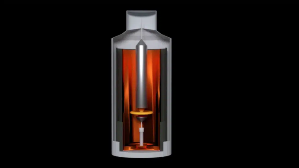
📊 FZ vs. CZ: Quick Comparison
| Parameter | FZ Method | CZ Method |
|---|---|---|
| Core Feature | Crucible‑free, ultra‑high purity | Crucible‑based, mature process, low cost |
| Oxygen/Carbon Content | Extremely low (O < 8×10¹⁵ atoms/cm³) | Relatively high (O ~10¹⁷–10¹⁸ atoms/cm³) |
| Resistivity Range | Ultra‑high (up to >20,000 Ω·cm) | Moderate (typically <100 Ω·cm) |
| Mechanical Strength | Lower (no oxygen pinning effect) | Higher (oxygen pins dislocations) |
| Maximum Diameter | Smaller (mainstream 200mm / 8‑inch) | Larger (300mm+ / 12‑inch+) |
| Primary Applications | High‑voltage power devices, detectors, RF | Integrated circuits, most photovoltaics |
| Market Share | ~5% | ~95% |
❓ What Is the Float Zone (FZ) Method and What Is Its Core Principle?
Answer: The Float Zone (FZ) method is a single‑crystal silicon growth technology that stands alongside the Czochralski (CZ) method. Its core advantage lies in its “crucible‑free” growth approach.
Core Principle: Floating + Zone Melting
The essence of the FZ method is captured in two key concepts:
| 개념 | Meaning | Key Enabler |
|---|---|---|
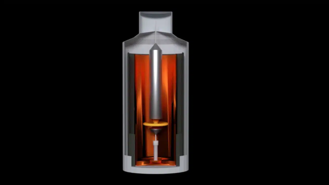
| Floating | A narrow molten zone is suspended between the feed polycrystalline rod and the grown single crystal below, without contacting any crucible or container | Surface tension of silicon melt + electromagnetic levitation force |
| Zone Melting | A radio‑frequency (RF) induction coil creates a molten zone; as the zone slowly moves upward, the melt below re‑crystallises onto the seed crystal with the same orientation | Precise temperature gradient and movement rate control |
Key point: The stable suspension of the molten zone is the technical core of the FZ method – it relies on the melt’s surface tension and the levitation effect of the RF electromagnetic field. This “contact‑free” state is the fundamental guarantee of ultra‑high purity.

❓ What Are the Key Process Steps of the FZ Method?
Answer: The FZ process consists of four core stages:
Step 1: Loading and Preparation
A high‑purity polycrystalline silicon rod is vertically mounted in the chamber, and a seed crystal with a specific crystallographic orientation (typically <100> or <111>) is fixed below it.
Step 2: Forming the Molten Zone
The RF induction coil is energised, melting the bottom of the polycrystalline rod to create a narrow molten zone that joins with the seed crystal below. Heating power must be precisely controlled to ensure zone stability.
Step 3: Crystal Growth
- The polycrystalline rod and seed crystal are slowly rotated to ensure uniform melting
- The molten zone is moved slowly upward (typically at 1–5 mm/min)
- As the melt exits the heating zone, it re‑crystallises onto the seed, growing a single crystal with the same orientation as the seed
Step 4: Complete Growth
The entire process requires precise control of temperature, movement rate, rotation speed, and other parameters, progressing through the standard growth stages:
- Seeding: Establishing a stable molten zone and growth interface
- Dash necking: Eliminating dislocations
- Shoulder formation: Expanding to the target diameter
- Constant‑diameter growth: The main body phase at steady diameter
- Tail‑off: Gradually reducing diameter to complete the crystal
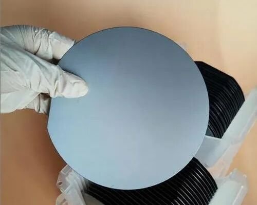
❓ What Are the Core Advantages of the FZ Method?
Answer: The advantages of the FZ method can be summarised as “one source, three indicators” – from the “crucible‑free” source, three key performance benefits follow.
Advantage 1: Ultra‑High Purity – No Crucible Contamination
By eliminating the quartz crucible, the FZ method fundamentally avoids crucible‑derived contamination. Especially critical is the extremely low content of light elements such as oxygen and carbon – FZ silicon achieves oxygen levels as low as 8×10¹⁵ atoms/cm³, one to two orders of magnitude lower than CZ silicon.
Advantage 2: Ultra‑High Resistivity – Up to >20,000 Ω·cm
High purity enables FZ silicon to achieve extremely high resistivity:
- Typical level: >1000 Ω·cm
- Premium level: >20,000 Ω·cm
- In contrast, CZ silicon is typically <100 Ω·cm
This ultra‑high resistivity makes it an ideal substrate material for high‑voltage power devices.
Advantage 3: Excellent Carrier Lifetime – Low Metallic Contamination
With extremely low metal impurity levels, FZ silicon exhibits significantly longer minority‑carrier lifetime than CZ silicon, contributing to improved device switching speed and efficiency.
One‑sentence summary: The FZ method trades the crucible for “three highs” – high purity, high resistivity, and high carrier lifetime.
❓ What Are the Main Limitations of the FZ Method?
Answer: Every technology has its trade‑offs. The limitations of the FZ method are reflected in four key aspects.
Limitation 1: Lower Mechanical Strength – No Oxygen Pinning Effect
The extremely low oxygen content is a double‑edged sword – FZ wafers lose the dislocation‑pinning effect of oxygen atoms, resulting in lower mechanical strength and greater susceptibility to breakage during processing and handling. This directly relates to the “shatter upon touch” behaviour discussed earlier: dislocations in FZ silicon propagate more readily at room temperature, reducing impact resistance.
Limitation 2: Limited Diameter – Reliance on Surface Tension
Since zone stability relies entirely on the melt’s surface tension, there is a physical upper limit to the diameter that FZ can achieve:
- Early stage: Limited to 150mm
- Current: 200mm (8‑inch) commercially available
- CZ method: 300mm (12‑inch) mature, advancing toward 450mm (18‑inch)
Limitation 3: Higher Production Cost – Stringent Equipment and Process Control
The FZ method demands extremely high precision in equipment, process control, and environmental cleanliness, resulting in significantly higher production costs than the CZ method.
Limitation 4: More Complex Doping – Additional Process Steps
Doping in the FZ method is not as straightforward as in the CZ process and typically requires additional steps:
- Neutron Transmutation Doping (NTD): Utilises nuclear reaction for uniform N‑type doping
- Gas‑phase doping: Introduces dopant gases during growth
One‑sentence summary: The price of the FZ method is “three lows” – low mechanical strength, low diameter ceiling, and low cost‑competitiveness.
❓ What Are the Key Application Areas of FZ Silicon?
Answer: Leveraging its ultra‑high purity, ultra‑high resistivity, and excellent carrier lifetime, FZ silicon is primarily used in high‑end applications with stringent material requirements.
| 적용 분야 | Typical Products | Key Performance Requirements |
|---|---|---|
| Power Electronics | High‑voltage rectifiers, thyristors, IGBTs | High resistivity, high breakdown voltage |
| High‑Performance Detectors | Photodetectors, radiation detectors, infrared detectors | Low leakage current, long carrier lifetime |
| RF & Communications | RF chips, key communication components | High purity, low loss |
| Optical Components | Terahertz lenses, window plates | High transparency to terahertz radiation |
| Specialty Photovoltaics | High‑efficiency solar cells for satellites | Long carrier lifetime, high conversion efficiency |
❓ How to Choose Between FZ and CZ Methods?
Answer: The choice between the two methods is essentially a trade‑off between “purity/performance” and “size/cost”.
| Scenario | Recommended Method | Reason |
|---|---|---|
| High‑voltage power devices (IGBT, thyristors) | FZ | Requires ultra‑high resistivity and breakdown voltage |
| High‑performance detectors and sensors | FZ | Requires extremely low leakage current and long carrier lifetime |
| RF/communication chips | FZ | Requires ultra‑high purity and low loss |
| Large‑scale ICs (CPU, memory) | CZ | Needs large‑diameter wafers, low cost, high mechanical strength |
| Conventional photovoltaics | CZ | Moderate purity requirements, cost‑sensitive |
| Specialty photovoltaics (satellites, aerospace) | FZ | Needs high efficiency, cost‑insensitive |
기사 출처:Jingge Semiconductor —초대형단결정 실리콘 소재 및 다결정 기둥상 실리콘 소재를 공급합니다. 당사의 제품은 반도체 에칭 공정에 사용되는 실리콘 부품의 가공을 위해 특별히 설계되었으며, 여기에는 직경 최대 650mm의 단결정 실리콘 링, 단결정 실리콘 웨이퍼, 기둥상 결정립 실리콘 링 및 다결정 실리콘 웨이퍼가 포함됩니다.