Single‑crystal silicon “shatters upon slight touch” at room temperature because of the combined effects of directional covalent bonds, high Peierls stress, and cleavage planes – external impact energy cannot be absorbed through “deformation” and must be released via “cleavage fracture.” This is the physical destiny of silicon as a hard and brittle material. In engineering practice, risks can be effectively mitigated by edge rounding, surface treatment, and adsorption clamping.
📊 Quick Overview of Shatter Causes and Countermeasures
| Cause Dimension | Physical Mechanism | Engineering Countermeasure |
|---|---|---|
| Atomic level | Strong directional covalent bonds (~2.3 eV/bond), no atomic slip | Precision machining to reduce stress concentration |
| Dislocation level | Extremely high Peierls stress, dislocations “frozen” at RT | Optimised stress distribution design |
| Fracture mechanics | Rapid crack propagation along {111} cleavage planes, microcrack stress amplification | Edge rounding + surface treatment to eliminate crack sources |
| Geometric size | High edge stress concentration in large thin‑walled parts (300–600 mm) | Large‑size precision machining capability |
❓ Why Do Silicon Components “Shatter upon Slight Touch”?
Answer: The brittle fracture of silicon at room temperature is determined by four physical mechanisms working together.
Level 1: Atomic Level – Directionality and High Strength of Covalent Bonds
Metals (e.g., aluminium, copper) are held together by metallic bonds; the electron gas acts like “glue” around the atomic nuclei, allowing atomic layers to slide past each other without fracture – giving them ductility. Single‑crystal silicon, however, has a diamond‑cubic structure with covalent bonds – each silicon atom forms a rigid tetrahedral structure with four surrounding silicon atoms, with a fixed bond angle of 109.5°.
Key point: Covalent bonds are highly directional. When an external force tries to displace atomic layers, these oriented strong bonds must be precisely broken. With a bond energy of about 2.3 eV per bond, atoms cannot release stress via “slip” like in metals at room temperature. Once stress accumulates, the only outcome is simultaneous bond rupture – cleavage fracture.
Level 2: Dislocation Level – Dislocations Are “Frozen” at Room Temperature
In metals, dislocations move easily at room temperature and absorb impact energy through plastic deformation. But in single‑crystal silicon, there exists an extremely high Peierls stress – think of it as the lattice “friction” against dislocation motion. At room temperature, atoms lack sufficient thermal vibration energy to help dislocations overcome the energy barrier.
Result: Dislocations are “frozen” or “pinned” in the silicon lattice – completely immobile. Since dislocations cannot “buffer” external forces through motion, the impact energy has nowhere to go and must be converted into the surface energy of newly formed cracks – hence, even a slight touch can cause instantaneous crack propagation and edge chipping.
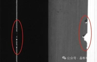
Level 3: Fracture Mechanics – Cleavage Planes and Microcrack Amplification
Cleavage plane {111}: The {111} planes have the largest inter‑planar spacing in silicon, meaning the weakest inter‑layer bonding. Once an edge is impacted, cracks propagate rapidly along {111} planes, like “tearing a stack of paper.”
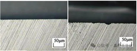
Griffith’s brittle fracture theory: Machining processes (cutting, grinding) inevitably leave micron‑scale microcracks (damage layers) at edges. According to fracture mechanics, the stress concentration at a crack tip is proportional to the crack length and inversely proportional to the tip radius. When the concentrated stress far exceeds the theoretical fracture strength of silicon, even a light touch can trigger catastrophic brittle chipping.
Level 4: Geometric Size Effect – Higher Risk for Large Parts
For large‑size (300–600 mm) silicon rings and electrodes, chipping is more prominent because:
- Thin‑wall effect: Large parts usually have thinner walls, making them prone to minor bending stresses during handling.
- Surface defect amplification: Larger diameters mean longer circumferential edges, increasing the probability of machining‑induced microcracks, and chipping risk rises exponentially.
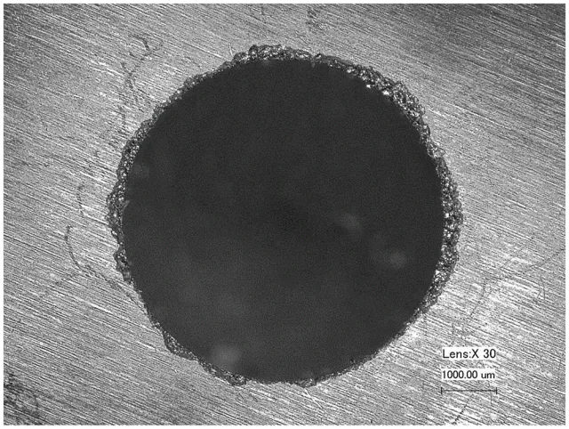
❓ How Can Chipping Be Mitigated in Engineering Practice?
Answer: Since the intrinsic brittleness of silicon cannot be changed, processing must “avoid” the risks through the following measures:
Measure 1: Edge Rounding (R‑chamfer or C‑chamfer)
Grinding sharp corners into R‑ or C‑chamfers effectively reduces the stress concentration factor at edges – this is the most effective geometric means of preventing chipping.
Measure 2: Chemical Etching to Remove the Damage Layer
After mechanical grinding, a brief chemical polish using a mixture of HF and HNO₃ can etch away several micrometres of the microcracked layer, eliminating the “crack sources.”
Measure 3: Adsorption Clamping
When machining thin‑walled rings, use porous ceramic vacuum chucks to avoid local stress points caused by mechanical clamping.
Measure 4: Large‑Size Precision Machining Capability
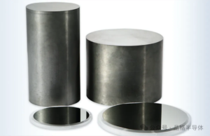
For 300–600 mm large silicon components, a complete process chain from material cutting, precision grinding to surface treatment is essential, supporting full custom processing including cutting, grinding, polishing, and drilling. Currently, single‑crystal silicon parts can reach 450 mm in diameter, and poly‑silicon products can exceed 600 mm.
❓ What Does This Mean for the Semiconductor Industry?
Answer: In semiconductor chip manufacturing, silicon components (such as rings and electrodes) are critical consumables in key processes like etching and diffusion, and their quality directly affects chip yield and cost.
Core value: By systematically understanding the chipping mechanisms of silicon components and addressing them from multiple dimensions – material purity, grain control, precision machining, and customised design – the industry can provide high‑reliability, long‑life, low‑cost silicon solutions.
Domestic silicon component manufacturers, represented by Jingge Semiconductor, are leveraging full‑melt ingot casting technology and Czochralski single‑crystal growth to achieve silicon purity above 99.99999% (total impurity concentration below 50 ppb). They are gradually breaking the long‑standing monopoly of international giants, enhancing the self‑reliance and cost competitiveness of key links in China’s semiconductor supply chain.
💎 요약
The physical destiny of silicon components – shattering upon slight touch – originates from the combined action of directional covalent bonds, high Peierls stress, and cleavage planes. Engineering solutions systematically address this through edge rounding, chemical etching to remove damage layers, and adsorption clamping.
| Cause | Engineering Countermeasure |
|---|---|
| Directional covalent bonds → no slip | Precision machining to reduce stress concentration |
| Dislocations frozen → no impact buffering | Optimised structural design |
| Cleavage planes + microcracks → crack propagation | Edge rounding + surface treatment |
| Large thin‑wall → edge stress concentration | Large‑size precision machining capability |
Final takeaway: Silicon “shatters upon slight touch” at room temperature because the directionality of covalent bonds and high Peierls stress together lock the path of atomic slip, so external impact cannot be absorbed as “deformation” and must be released as “cleavage fracture.” Understanding this physical destiny and applying targeted engineering measures is the key to improving the reliability of silicon components.
Article source: Jingge Semiconductor — Supplies ultra‑large‑size single‑crystal silicon materials and polycrystalline columnar‑grained silicon materials. Our products are specifically designed for the processing of silicon components used in semiconductor etching applications, including single‑crystal silicon rings, single‑crystal silicon wafers, columnar‑grained silicon rings, and polycrystalline silicon wafers, with diameters up to 650 mm.