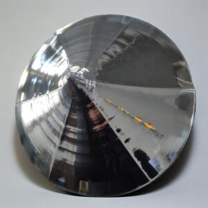
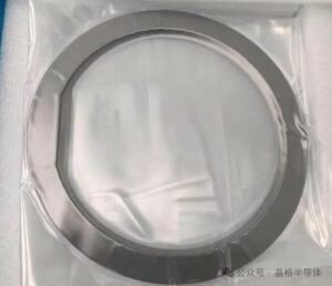
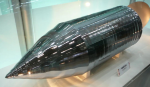
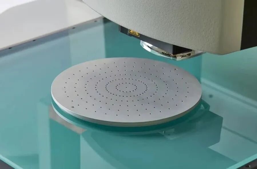
The showerhead (gas distribution plate) is the core gas distribution component in plasma etchers and CVD equipment. It features tens of thousands of micro‑holes with aperture precision within ±1 μm and wall roughness Ra < 0.2 μm. Innovations such as ultrasonic‑assisted drilling, femtosecond laser machining, and hybrid processes are pushing showerhead micro‑hole drilling toward higher precision, greater efficiency, and broader material adaptability – making it a critical enabler for the self‑reliance of the semiconductor supply chain.
📊 Showerhead Micro‑Hole Drilling at a Glance
| Aspect | Key Data / Requirement |
|---|---|
| Market Size | ~$2.5B globally in 2023, projected $3.5B by 2028; China market growing at 25% CAGR |
| Number of Holes | ~100,000 holes for a 12‑inch wafer |
| Hole Diameter | 0.2–6.0 mm; advanced processes trending toward 30–100 μm |
| Aspect Ratio | Up to 20:1 or even >55:1 |
| Hole Diameter Uniformity | ≤ ±0.5 μm |
| Wall Roughness | Ra < 0.2 μm |
| Primary Materials | Single‑crystal silicon, CVD‑SiC, aluminium alloy (6061‑T6) |
| Market Landscape | Dominated by AMAT (US) and TEL (Japan); localisation rate in China <30% |
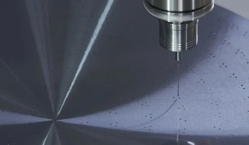
❓ What Is a Showerhead and Why Is It So Important?
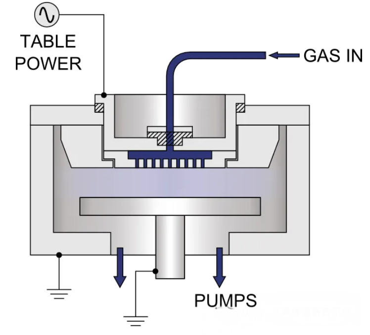
Answer: The showerhead (gas distribution plate) is the core gas distribution component in plasma etchers and chemical vapour deposition (CVD) equipment.
During wafer processing, process gases pass through the micro‑hole array on the showerhead surface and are uniformly delivered onto the wafer. Its performance directly determines:
- Uniformity of thin‑film deposition
- Precision of etching
- Stability of plasma distribution
A single showerhead can cost over $60,000 (40万人民币). The root of this high cost lies in its extremely demanding manufacturing requirements – thousands of micro‑holes with stringent demands on diameter accuracy, consistency, and internal wall smoothness.
Market data: According to Techcet, the global semiconductor showerhead market was valued at approximately $2.5 billion** in 2023 and is projected to reach **$3.5 billion by 2028. The Chinese market is leading the Asia‑Pacific region with an impressive 25% growth rate. However, the high‑end segment is currently dominated by Applied Materials (AMAT) of the US and Tokyo Electron (TEL) of Japan, with China’s localisation rate below 30% .
❓ What Are the Core Challenges in Showerhead Micro‑Hole Drilling?
Answer: Showerhead micro‑hole drilling faces three major challenges, each pushing the limits of current manufacturing technology.
Challenge 1: Hard‑and‑Brittle Materials
Showerhead materials fall into two main categories:
| Material Type | Typical Materials | Characteristics | Applications |
|---|---|---|---|
| Metals | Aluminium alloy (6061‑T6) | Good thermal conductivity, corrosion resistance, easy to machine | Mid‑to‑low‑end processes |
| Non‑metals | Single‑crystal silicon, CVD‑SiC, AlN, quartz glass | High‑temperature resistance (>600°C), chemical inertness, thermal expansion matching | High‑end semiconductor processes |
Single‑crystal silicon and silicon carbide are the most common materials for semiconductor showerheads. However, they are extremely sensitive to machining – edge chipping at the hole entrance is a major issue, and tool wear is significant.
Challenge 2: Ultra‑High Aspect Ratios
Micro‑holes can have aspect ratios of 20:1 or even >55:1, making chip evacuation extremely difficult. For example, a hole of D0.45 mm × 24.75 mm has an aspect ratio of 55:1 – equivalent to drilling a 25‑mm‑deep hole with a diameter less than 0.5 mm.
| Design Parameter | Typical Value | Extreme Requirement |
|---|---|---|
| Hole Diameter | 0.2–6.0 mm | 30–100 μm (advanced nodes) |
| Hole Density | 300–1200 holes/cm² | — |
| Hole Wall Verticality | ≥89.5° | 90°±0.5° (advanced nodes) |
| Diameter Uniformity | ≤ ±0.5 μm | — |
Challenge 3: Batch Consistency
Tens of thousands of holes must maintain diameter deviations within ±0.5 μm. Minor vibrations or tool wear during processing can easily introduce taper or over‑sizing defects.
For sub‑3nm processes, film thickness uniformity across the wafer must be controlled within ±0.1 nm, which requires showerhead hole diameter tolerances below ±1 μm and wall roughness Ra < 0.2 μm. Any slight burr or flow deviation can cause non‑uniform etching/deposition, directly scrapping the entire wafer.
❓ Why Do Traditional Drilling Technologies Fall Short?
Answer: Traditional methods have clear limitations in precision, efficiency, and material adaptability.
Mechanical Drilling
| Aspect | Limitation |
|---|---|
| Precision | Tool wear leads to diameter deviations of up to 5 μm |
| Material Adaptability | Cannot effectively machine hard materials like CVD‑SiC |
| Hard‑Brittle Issues | Insufficient rigidity and uneven cutting force cause edge chipping |
Electrical Discharge Machining (EDM)
| Aspect | Limitation |
|---|---|
| Heat‑Affected Zone (HAZ) | Recast layer and micro‑cracks on hole walls require post‑acid cleaning |
| Efficiency | A single 12‑inch showerhead requires >10 tool changes and >20 hours of processing |
| Material Limitation | Only applicable to conductive metals |
Chemical Etching
- Isotropic etching leads to tapered hole walls, failing verticality requirements
- Resolution limits of photoresist cannot meet the requirements for holes <30 μm

❓ How Are Innovative Drilling Technologies Breaking Through?
Answer: In recent years, ultrasonic‑assisted drilling, femtosecond laser machining, and hybrid processes are systematically overcoming the core bottlenecks of showerhead micro‑hole drilling.
Technology 1: Ultrasonic‑Assisted Drilling
Principle: High‑frequency micro‑vibration (16–60 kHz) is applied to the drill bit. The bit periodically contacts and separates from the workpiece, reducing cutting forces by about 40%.
Typical application – Single‑crystal silicon showerhead, D0.45 mm × 24.75 mm (aspect ratio 55:1):
| Metric | Result |
|---|---|
| Tool Life | One PCD drill bit can continuously machine >2,000 ultra‑deep micro‑holes |
| Hole Entrance Quality | No visible chipping |
| Hole Roundness | 0.003 mm |
| Wall Roughness | From Sa 6.540 μm to Sa 0.013 μm (99.8% reduction) |
Core advantages: Suppresses micro‑cracks, improves surface quality, reduces burrs, lowers cutting forces, and extends tool life.
Technology 2: Femtosecond Laser Drilling
Principle: Femtosecond lasers (pulse width <10⁻¹⁵ s) enable “cold processing” with virtually no heat‑affected zone (HAZ width ≤0.2 μm).
| Metric | Performance |
|---|---|
| Diameter Precision | ≤ ±1 μm |
| Wall Roughness | Ra < 0.2 μm |
| Materials | CVD‑SiC, AlN, and other hard non‑metals |
| Efficiency | One machine can process 128 holes simultaneously, 15× faster than mechanical drilling |
Advantages and trade‑offs:
- ✅ High precision, broad material compatibility, dramatically improved efficiency
- ⚠️ Equipment cost >$5 million, processing cost 3× that of EDM
- ⚠️ Daily output: only 5–10 pieces of 12‑inch showerheads per machine
Technology 3: Hybrid Process (Laser + Grinding)
To overcome the limitations of any single method, the industry is adopting a “laser roughing + diamond grinding finishing” approach:
- Laser roughing: Rapidly creates the micro‑hole array
- Diamond grinding: Precision‑polishes the hole walls, eliminating taper and burrs from laser processing
Application case: Anhui Boxin Micro has achieved mass production of 12‑inch showerheads using this hybrid process, with hole wall verticality reaching 90°±0.5°, meeting the requirements of 5nm nodes.
Technology 4: Cutting Tool Breakthroughs
Micro‑hole drilling demands extremely high‑performance cutting tools. Key advancements include:
| Tool Type | Core Technology | Advantages |
|---|---|---|
| PCD Micro‑Drill | Polycrystalline diamond material | Extremely wear‑resistant, long tool life, excellent diameter consistency |
| DLC‑Coated Drill | Diamond‑like carbon coating (sp³ up to 60 GPa) | Low friction, prevents chip adhesion, reduces cutting resistance |
| Through‑Coolant Drill | Cutting fluid delivered internally to the cutting point | Forced chip evacuation, lubrication, and cooling; ideal for ultra‑deep holes |
Specialist manufacturers such as Japan’s ATOM have developed mature DLC‑coated and through‑coolant drill solutions, significantly improving the quality and efficiency of ultra‑deep micro‑hole drilling.
❓ How Are Showerhead Micro‑Holes Inspected and Quality‑Controlled?
Answer: The extreme precision required demands a multi‑dimensional, full‑process inspection system.
| Inspection Technology | Inspection Content | Features |
|---|---|---|
| CMM (Coordinate Measuring Machine) | Hole diameter, pitch, flatness | Contact‑based, suitable for batch sampling |
| AOI (Automated Optical Inspection) | Hole roundness, foreign matter | Non‑contact, rapid inspection |
| X‑ray CT (Computed Tomography) | 3D imaging of internal channels; hidden defects (cracks, voids) | Ideal for complex showerhead structures |
| 3D Profilometer (White‑light Interferometry) | Diameter, roundness, taper deviation | Non‑contact, diameter uniformity standard deviation σ≤0.5 μm |
| AI Vision Inspection | Rapid identification of anomalous holes | Deep‑learning algorithms enable 100% inspection of tens of thousands of holes |
❓ What Are the Future Trends in Showerhead Micro‑Hole Drilling?
Answer: Current development is moving toward higher precision, greater efficiency, and broader material adaptability.
Trend 1: Pushing Precision Limits
As advanced nodes move toward 3nm and below, micro‑hole precision requirements have already reached the sub‑micron level. Advanced techniques like femtosecond laser machining are the key path to achieving this.
Trend 2: Diversification of Process Routes
Mechanical drilling, ultrasonic‑assisted drilling, femtosecond laser, and hybrid processes each have their strengths. Selecting the optimal solution based on material, hole size, and cost will become industry standard.
Trend 3: Intelligent Quality Control
The integration of AI vision inspection, X‑ray CT, and other advanced techniques will enable 100% full inspection of tens of thousands of holes, fundamentally ensuring product reliability.
💎 Summary
Showerhead micro‑hole drilling is a complex system engineering challenge that integrates hard‑and‑brittle material machining, ultra‑deep micro‑hole drilling, and ultra‑high precision batch consistency:
| Challenge | Innovative Solution | Key Result |
|---|---|---|
| Chipping in hard‑brittle materials | Ultrasonic‑assisted drilling + PCD micro‑drill | 40% cutting force reduction; no visible chipping |
| Ultra‑high aspect ratio (55:1) | Ultrasonic machining + through‑coolant drill | >2,000 holes per tool; 99.8% roughness reduction |
| Batch uniformity (±0.5 μm) | Femtosecond laser + hybrid (laser+grinding) | Verticality 90°±0.5°; meets 5nm node requirements |
| High‑throughput inspection | AI vision + X‑ray CT + 3D profilometry | 100% full inspection; σ≤0.5 μm |
Final conclusion: From ultrasonic‑assisted drilling to femtosecond lasers, from PCD micro‑drills to hybrid processes – each technological breakthrough pushes the boundaries of semiconductor manufacturing precision. Mastering the core technologies of showerhead micro‑hole drilling is not just about manufacturing a single component; it is about the self‑reliance and long‑term development of the semiconductor supply chain.
Article source: Jingge Semiconductor — Supplies ultra‑large‑size single‑crystal silicon materials and polycrystalline columnar‑grained silicon materials. Our products are specifically designed for the processing of silicon components used in semiconductor etching applications, including single‑crystal silicon rings, single‑crystal silicon wafers, columnar‑grained silicon rings, and polycrystalline silicon wafers, with diameters up to 650 mm.