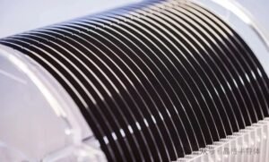
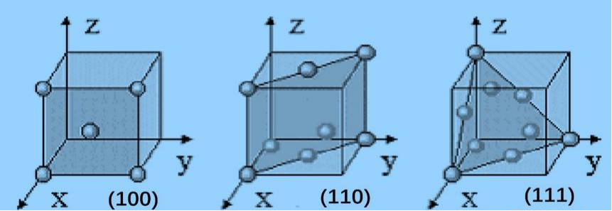
In semiconductor manufacturing, the choice of wafer crystal orientation directly determines the “genetic expression” of chip performance. Single-crystal silicon has a diamond cubic structure; when the cutting direction forms different angles with the crystal axes, crystal planes with specific atomic arrangements are exposed. Among the three major orientations — 〈100〉, 〈110〉, and 〈111〉 — the 〈100〉 orientation dominates with a market share exceeding 93% (reaching 98% for 12‑inch wafers), making it the absolute mainstream of the semiconductor industry. This near‑monopoly position is the result of a combination of electrical performance, process compatibility, mechanical workability, and industrial ecosystem.
1. Electrical performance: dual advantages of interface state density and carrier mobility
1.1 Lowest interface state density
CMOS devices are extremely sensitive to interface states, and the 〈100〉 surface has the lowest state density among the three main orientations. This low density ensures stable threshold voltage in MOS devices, which is the core reason why 〈100〉 is the substrate of choice for MOS integrated circuits. From the atomic perspective, the 〈100〉 surface has a square grid atomic arrangement and the lowest dangling bond density, allowing the (100)/(100) interface with the gate oxide to achieve the highest quality. In contrast, although the 〈111〉 surface has the highest atomic packing density (7.83×10¹⁴ atoms/cm²), its dangling bond density is higher, leading to significantly higher interface state density – precisely why 〈111〉 is typically used for bipolar devices rather than MOS devices.
1.2 Highest electron mobility
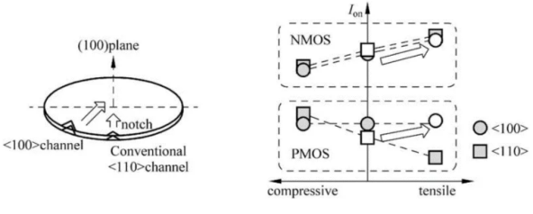
In the silicon lattice, the atomic arrangement along the 〈100〉 direction causes the weakest lattice scattering for electrons moving in the channel. The electron mobility on 〈100〉 silicon can reach 1450 cm²/(V·s), about 35% higher than that on 〈111〉. In early semiconductor circuits, nMOS devices dominated logic operations, and pMOS devices served only as complementary structures. The performance advantage of nMOS on 〈100〉 substrates was sufficient to cover overall circuit requirements, so throughout mature nodes from 0.18 μm to 40 nm, 〈100〉 remained the industry standard. According to the International Technology Roadmap for Semiconductors, 92% of logic chips worldwide use 〈100〉 wafers.
1.3 High‑quality thermal oxide
The oxidation rate on the 〈100〉 plane is isotropic, which facilitates the formation of a uniform gate oxide layer with thickness variation controlled within ±2%. The defect density of the thermal oxide is reduced by about 40% compared to other orientations. A high‑quality gate oxide is essential for MOS device reliability, and this advantage is irreplaceable in logic chip manufacturing.
2. Process compatibility: full adaptability from crystal growth to device fabrication
2.1 Anisotropic etching and texturing advantage
In alkaline solutions (e.g., KOH, TMAH), silicon exhibits vastly different etch rates for different orientations. The etch rate of the 〈100〉 plane is more than ten times that of the 〈111〉 plane – some studies even report a ratio of up to 400. This property has tremendous engineering value: for 〈100〉 wafers, anisotropic etching produces countless tetragonal pyramids (i.e., textured structures) on the surface, with 〈111〉 facets. This texture reduces surface reflectance to about 11% and enhances light trapping, significantly improving solar cell efficiency. The photovoltaic industry therefore prefers 〈100〉. The 〈111〉 orientation, being close‑packed and chemically stable, is hardly etched in alkaline solutions and cannot achieve this texturing, which is a key reason for its marginalization in photovoltaics.
2.2 Crystal growth feasibility
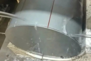
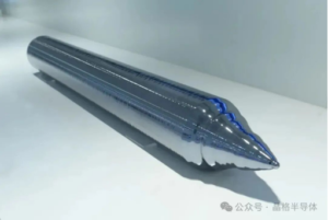
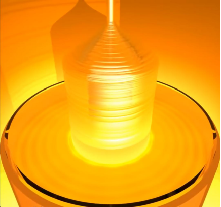
Although 〈111〉 offers more stable growth behaviour during pulling, 〈100〉 excels in avoiding defects. Studies have shown that in directional solidification, 〈100〉 is the most favourable growth direction, more effectively preventing defect clusters above seed gaps compared to 〈111〉 and 〈110〉. Early 〈100〉 crystals did suffer from low yield and high dislocation density, but these issues have been resolved through optimised thermal system design and process control. The 〈100〉‑grown silicon ingot has a cylindrical shape with four distinct edges, which facilitates subsequent wafer orientation and processing.
2.3 Epitaxy and doping compatibility
High‑quality epitaxial growth can be achieved on 〈100〉 substrates; for example, the dislocation density of GaN epitaxy on 〈100〉 can be controlled below 10⁶ cm⁻². In doping, impurity atoms can be incorporated into the lattice in different ways depending on the orientation. The symmetry of the 〈100〉 orientation allows more uniform and controllable doping profiles, which is critical for integrated circuit manufacturing.
2.4 Mechanical workability
The Vickers hardness of 〈100〉 is about 11.5 GPa, the lowest among the three major orientations. This means 〈100〉 wafers are easier to cut, grind, and polish, with lower tool wear and higher processing efficiency. In contrast, 〈111〉 has the highest hardness (~13.5 GPa) and requires harder diamond wire (50‑70 μm grit) and a 20% slower feed rate during cutting. From a cost perspective, 〈100〉 wafers are cheaper than 〈110〉 and 〈111〉 wafers.
3. Industrial ecosystem: positive feedback of standardisation and scale effects
3.1 Entrenchment in international standards
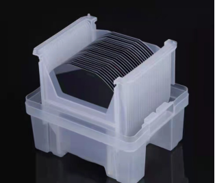
The 〈100〉 orientation has been codified in numerous international standards. SEMI standards clearly define the flat specifications for 〈100〉 wafers: if the minor flat is 180° from the primary flat, it is n‑type 〈100〉; if 90°, it is p‑type 〈100〉. For 200 mm wafers, the notch orientation is specified as 〈110〉 ±1°. SEMI MF1725 also provides analytical methods for orientation integrity of ingots grown in 〈111〉 and 〈100〉 directions. National standards such as GB/T 1555‑2023 have similarly established complete testing and quality control frameworks around 〈100〉.
2.2 Full supply chain adaptation
From crystal growth equipment, cutting tools, lapping and polishing consumables, to lithography, etching, and deposition tools – the entire semiconductor supply chain has been deeply optimised for 〈100〉. Hundreds of millions of silicon wafers produced globally each year are predominantly 〈100〉. Memory chips such as DRAM, SRAM, and flash memory also mainly use 〈100〉 wafers. This scale further reduces 〈100〉 wafer costs, creating a positive feedback loop of “higher volume → lower cost → more adoption”.
4. Challenges and evolution of 〈100〉
〈100〉 is not without drawbacks. Its biggest weakness is low hole mobility – on 〈100〉 substrates, hole mobility is only 250‑450 cm²/(V·s), less than one‑third of electron mobility. As process nodes entered 28 nm and below, pMOS performance became a bottleneck. The industry has developed several approaches:
- Strained silicon engineering: introducing biaxial tensile strain via SiGe epitaxy to further increase electron mobility on 〈100〉 to ~1600 cm²/(V·s).
- Hybrid orientation technology (HOT): proposed by Intel in 2021, this locally creates 〈110〉 regions on a 〈100〉 substrate, improving nMOS and pMOS carrier mobilities by 25% and 10%, respectively.
- Orientation switching: at 28 nm and below, some manufacturers have started adopting 〈110〉 substrates because hole mobility on 〈110〉 can reach 600‑800 cm²/(V·s), 1.5‑2 times that of 〈100〉.
Nevertheless, 〈110〉 holds only about 4.5% of the overall market, and 〈111〉 less than 2.5%. 〈100〉 remains unassailable in mainstream areas such as logic, 3D NAND, and CIS image sensors.
Conclusion
〈100〉 has become the “only choice” of the semiconductor industry because of the triple superposition of optimal electrical performance (lowest interface state density, highest electron mobility), best process compatibility (anisotropic etching for texturing, uniform oxidation, ease of machining), and most mature industrial ecosystem (standardisation, mature supply chain, lowest cost). As noted in crystal growth research, although the 〈111〉 plane offers stable growth habits, other low‑index planes such as 〈100〉 and 〈110〉 are increasingly used – and among them, 〈100〉 holds an unshakable leading position.
Article source: Jingge Semiconductor — Providing ultra-large-size monocrystalline silicon materials, polysilicon columnar-grain materials, and custom processing of Si parts, silicon components, silicon targets, silicon electrodes, silicon rings, silicon barrels, silicon wafers, etc.