1. At Room Temperature (Brittle Region): Dislocations Are the “Culprit of Fracture,” Reducing Strength
At room temperature, monocrystalline silicon is a typical brittle material. In this case, the effect of dislocations on mechanical strength manifests as “embrittlement”:
- Dislocation pile-up leads to stress concentration: Under external stress, dislocations move along slip planes. However, when they encounter grain boundaries, impurity precipitates (such as oxygen precipitates), or other dislocations, they become “pinned.” This causes subsequent dislocations to pile up at these sites, generating enormous stress concentration.
- Microcrack nucleation: When this stress concentration reaches the critical fracture strength of atomic bonds, microcracks nucleate directly at the dislocation pile-up sites (following Griffith’s theory of brittle fracture).
- Result: The higher the dislocation density, the greater the probability of microcrack nucleation, and the material’s fracture strength and bending strength drop sharply. During wafer slicing or edge beveling, silicon wafers with high dislocation density are highly prone to chipping and breakage.
2. At High Temperatures (Plastic Region): Dislocations Are the “Carriers of Deformation,” Reducing Yield Strength
When the temperature exceeds 700°C, the kinetic energy of silicon atoms increases, and dislocations gain sufficient thermal activation energy to slip and climb. At this stage:
- Yield strength drops significantly: The critical resolved shear stress (CRSS) required for dislocation motion decreases sharply with rising temperature. Consequently, during high-temperature processes (such as epitaxial growth), even a very small internal thermal stress can trigger massive dislocation slip.
- Creep and warpage: Dislocation motion induces macroscopic plastic deformation (i.e., “slip”), causing irreversible bending of the silicon wafer (increased warpage). This means that the resistance to thermal deformation—i.e., mechanical strength—deteriorates markedly.
3. In-Depth Mechanism Analysis: Why Does This Happen?
To answer this question, we must start from the fundamental physics, primarily involving covalent bond characteristics and Peierls stress:
- Extremely high lattice friction (Peierls stress): Silicon has a diamond cubic structure, and its covalent bonds are highly directional. For a dislocation to move through the lattice, Si–Si covalent bonds must be broken and reformed. At room temperature, thermal energy is insufficient to help atoms overcome this high energy barrier, so dislocations are “frozen” in the lattice. At this point, dislocations act like internal sharp defects, which only trigger brittle fracture.
- Thermal activation assistance: At high temperatures, atomic thermal vibrations intensify, and the applied stress helps dislocations overcome the energy barrier. Dislocations can now move, dissipating the work done by external forces. However, this dissipation comes at the cost of dimensional stability—macroscopically manifested as a sharp deterioration in mechanical strength and deformation resistance.
4. Engineering Impact Quantification
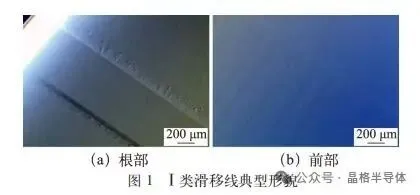
Although high dislocation density reduces fracture strength at room temperature, the number one killer of mechanical strength in IC manufacturing is usually not individual dislocations, but dislocation arrays (slip bands). When slip occurs, hundreds or thousands of dislocations slide simultaneously along the {111} crystal planes, forming topographic steps of several micrometers or even tens of micrometers within the silicon wafer. This directly leads to:
- Excessive total thickness variation (TTV), causing the wafer’s geometric flatness to exceed specifications.
- Edge chipping during subsequent grinding and polishing processes.
In summary:
Dislocations are like the “Achilles’ heel” of monocrystalline silicon’s mechanical properties—at room temperature, they are sources of brittle fracture; at high temperatures, they are the medium for plastic deformation. Both mechanisms significantly weaken the material’s ability to resist external forces or thermal stress.
For etching components that are repeatedly subjected to high-temperature bombardment and cooling cycles in plasma etchers, if the initial monocrystalline ingot has uneven dislocation density, slip is likely to occur under these thermal cycling stresses, causing electrodes or showerheads to warp and fail. Therefore, supplying high-purity, low-dislocation-density monocrystalline ingots is a prerequisite for ensuring their mechanical lifespan.
Article source: Jingge Semiconductor — Providing ultra-large-size monocrystalline silicon materials, polysilicon columnar-grain materials, and custom processing of Si parts, silicon components, silicon targets, silicon electrodes, silicon rings, silicon barrels, silicon wafers, etc.