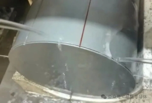
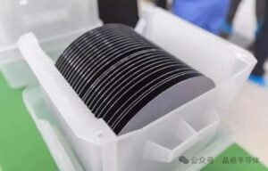
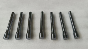
Monocrystalline silicon, as the foundational functional material for the semiconductor and photovoltaic industries, has its crystal integrity directly determining the electrical performance and service life of devices. Dislocations, as one-dimensional lattice defects, are key factors affecting minority carrier lifetime, leakage current, and mechanical strength. Among the numerous dislocation characterization techniques, chemical etching has been the most widely adopted dislocation detection method in both industry and academia since the mid-20th century, owing to its advantages of simple equipment, intuitive results, and quantitative statistics. However, the effectiveness of this method is no accident—it is rooted in the profound intrinsic connection between the crystallographic nature of dislocations and the physicochemical laws of etching reactions. This article will systematically elaborate, starting from the fundamental crystallographic characteristics of dislocations, the complete mechanism system by which chemical etching enables dislocation detection, covering the entire chain from atomic-scale distortion to the macroscopic morphology of etch pits.
1. Fundamental Crystallographic Characteristics of Dislocations
1.1 Structural Types and Geometric Description of Dislocations
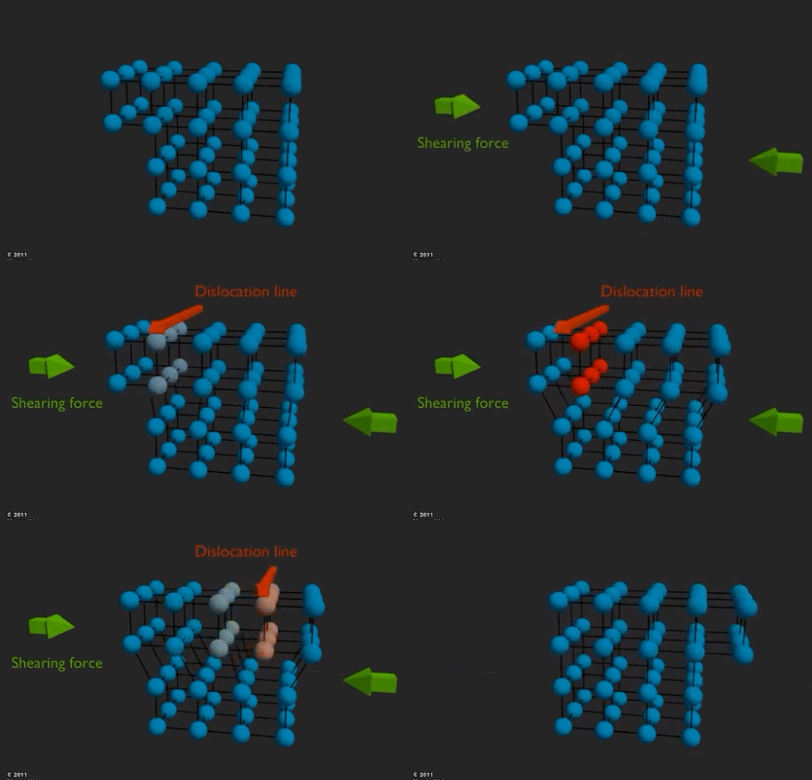
Monocrystalline silicon has a diamond cubic structure, in which the atomic arrangement consists of two face-centered cubic lattices offset by 1/4 along the body diagonal. In this highly ordered periodic field, a dislocation is a linear lattice defect characterized by one-dimensional misalignment of atomic arrangement along a certain line (the dislocation line). According to the geometric relationship between the dislocation line and the Burgers vector, dislocations can be divided into two basic types:
- Edge dislocation: The Burgers vector is perpendicular to the dislocation line. Its physical picture is that there exists an extra half-plane of atoms inserted into the crystal, forming a line—the dislocation line—at the edge of the insertion. The lattices on both sides of the half-plane respectively bear compressive stress (on the side of the extra atomic plane) and tensile stress (on the missing side), causing significant elastic displacement of atoms around the dislocation line.
- Screw dislocation: The Burgers vector is parallel to the dislocation line. It can be viewed as a shear along a certain crystal plane, causing the plane to arrange in a spiral step-like manner around the dislocation line, with atoms undergoing continuous rotational displacement along the path encircling the dislocation line.
- Mixed dislocation: In actual crystals, mixed dislocations, where the Burgers vector is neither perpendicular nor parallel to the dislocation line, are more common. These can be decomposed into edge and screw components.
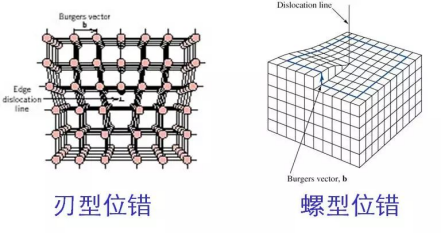
In silicon crystals, dislocations typically extend along the <110> direction, with a Burgers vector of a/2<110> (where a is the lattice constant), and a slip plane of {111}. This specific slip system determines the crystallographic orientation characteristics of dislocation etch pits.
1.2 Lattice Distortion Field Around Dislocations
Whether edge or screw dislocation, there exists significant lattice distortion around the dislocation line. Atoms deviate from their ideal equilibrium positions, with bond lengths being stretched or compressed, thereby generating a local elastic strain field. This distortion means that atoms in the dislocation region possess higher internal energy (strain energy) than those in the perfect lattice. From a thermodynamic perspective, regions of higher energy exhibit greater chemical activity—atoms are in a metastable state and more readily participate in chemical reactions.
It is precisely this physical characteristic of “high strain energy” that constitutes the thermodynamic basis for the selective etching of dislocations by chemical etching.
1.3 Sources of High Chemical Activity in Dislocation Regions
The lattice distortion around dislocations directly leads to enhanced chemical activity in three aspects:
- Reduced bond energy: The deviation of atomic spacing from the equilibrium bond length causes Si-Si covalent bonds to be stretched or compressed, raising the bond potential energy. At the dislocation core, some atoms form “dangling bonds” or incomplete bonding, placing them in a higher energy state.
- Electrochemical potential difference: The strain field alters the local electronic band structure, causing the Fermi level at the dislocation core region to differ from that of the perfect lattice, forming additional energy levels (deep levels) in the semiconductor. This gives dislocation sites a different electrochemical potential in the etching solution, making them the anodic regions that preferentially react.
- Impurity segregation effect: The stress field of dislocations can capture impurity atoms (such as oxygen, carbon, and metal ions), forming Cottrell atmospheres. Impurity segregation further alters the local chemical composition and bonding state, making the dissolution behavior of these regions even more distinct from the matrix.
In summary, atoms around dislocations are in a thermodynamically metastable state, with their dissolution activation energy significantly lower than that of the perfect lattice. This difference (ΔE_a), typically on the order of 0.1–0.3 eV, though seemingly small, produces an exponential rate difference in the kinetic competition of chemical etching.
2. Physicochemical Mechanism of Dislocation Detection by Chemical Etching
2.1 Thermodynamic Basis of Preferential Etching
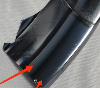
The core principle of dislocation detection by chemical etching can be summarized as “distortion stores energy, etching favors distortion.” When a monocrystalline silicon sample is immersed in a specific chemical etchant, the chemical components in the etchant (such as oxidants and complexing agents) react chemically with the silicon surface, dissolving silicon atoms. However, this dissolution process does not proceed uniformly—atoms at the dislocation emergence points (i.e., the intersections of dislocation lines with the crystal surface), being in a high strain energy state, have a dissolution activation energy significantly lower than that of atoms in the perfect lattice regions. In other words, atoms at dislocations are more readily “attacked” and dissolved by the etchant.
2.2 Chemical Composition and Function of Etchants
The components of chemical etchants typically fall into three major categories:
- Oxidants: Such as concentrated HNO₃, CrO₃ solution, or K₂Cr₂O₇ solution, responsible for oxidizing silicon atoms to SiO₂.
- Complexing agents: Such as hydrofluoric acid (HF), responsible for dissolving the oxidation products to sustain the reaction.
- Diluents: Such as deionized water or glacial acetic acid, used to adjust the reaction rate and etching selectivity.
The proportion of oxidizing components in the etchant determines the macroscopic etching effect: a higher proportion of oxidants produces a stronger polishing effect, suitable for surface planarization; a higher proportion of complexing and diluting components favors preferential etching, enabling prominent display of dislocations and other defects.
2.3 Formation and Evolution of Etch Pits
During the preferential etching process, the dissolution rate at dislocation emergence points is much higher than that in the surrounding perfect lattice regions. As etching proceeds, the dislocation points are rapidly etched downward, gradually forming an etch pit with a specific geometric shape.
The final morphology of the etch pit is determined by two factors:
First, the anisotropy of the crystal structure. Monocrystalline silicon exhibits significantly anisotropic etching rates due to different atomic packing densities on different crystal planes. Specifically:
- On the {111} crystal plane, dislocation etch pits appear as triangles;
- On the {100} crystal plane, dislocation etch pits appear as squares;
- On the {110} crystal plane, dislocation etch pits appear as cuboids.
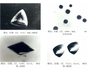
Second, the type of etchant. The morphology of etch pits on the same crystal plane may also differ with different etchants. For example, in the non-preferential etchant Dash etchant, dislocation pits on the {111} plane of silicon single crystals appear as circular depressions; whereas in crystallographically preferential etchants, the pits on the {111} plane appear as triangular pyramids. The duration of etching also affects the pit morphology—as etching time increases, triangular pits may gradually evolve into circular depressions.
2.4 The “One-to-One Correspondence” Between Etch Pits and Dislocations
The fundamental prerequisite for chemical etching to serve as a quantitative detection method is that there exists a strict “one-to-one correspondence” between etch pits and dislocations. As early as 1964, Hong Jing and colleagues published a classic study titled “The Correspondence Between Dislocations and Etch Pits in Silicon” in Acta Physica Sinica. Through a series of rigorous experimental methods, this study proved that the etch spots obtained by chemical etching indeed correspond one-to-one with dislocations. These verification methods included:
- Prolonged etching: Observing the evolution of etch pits over time;
- Layer-by-layer etching and alternating polishing: Confirming that the depth extension of etch pits is consistent with the spatial orientation of dislocation lines;
- Cleavage plane correspondence: Observing the correspondence of etch spots on cleavage planes;
- Small-angle grain boundary observation: The geometric characteristics of dislocation arrangement at small-angle grain boundaries perfectly match the arrangement of etch spots;
- Deformed sample observation: After bending or indentation deformation, the arrangement of etch spots is consistent with the crystallographic laws of dislocation slip;
- Quantitative relationship between curvature radius and dislocation density: The curvature radius of bent samples and the dislocation density satisfy the mathematically predicted relationship.
These experiments cross-validated the correspondence between etch pits and dislocations from multiple independent perspectives, laying a solid experimental foundation for the quantitative application of chemical etching.
Article source: Jingge Semiconductor — Providing ultra-large-size monocrystalline silicon materials, polysilicon columnar-grain materials, and custom processing of Si parts, silicon components, silicon targets, silicon electrodes, silicon rings, silicon barrels, silicon wafers, etc.