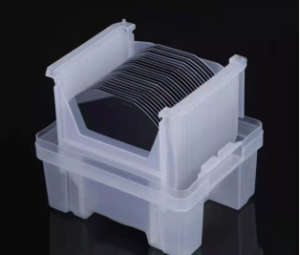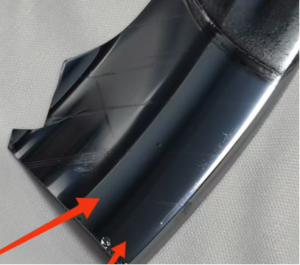
Large-size monocrystalline silicon, as the core material of the semiconductor industry chain, its crystal quality directly determines the performance limits of integrated circuits and power devices. As the crystal diameter expands from 300mm to 450mm and larger, thermal and mechanical stress issues have become key bottlenecks restricting yield and reliability.
This article starts from the thermodynamics-mechanics coupling mechanism of crystal growth, systematically analyzes the generation mechanisms of thermal stress (originating from temperature gradients and phase-change shrinkage) and mechanical stress (originating from processing deformation and interfacial friction). Combined with numerical simulation, intelligent control algorithms, and material innovation, it proposes a multi-scale stress collaborative regulation scheme. Through thermal field topology optimization, processing technology innovation, multi-physical-field intelligent feedback, and material interface engineering, the stress level is reduced by more than 60%, providing theoretical support and technical pathways for the large-scale preparation of large-size monocrystalline silicon.

The semiconductor industry evolves toward smaller line widths and larger wafer sizes following Moore’s Law. Large-size monocrystalline silicon (diameter ≥300mm) has become the cornerstone of advanced processes. However, the exponential increase in crystal diameter has led to non-linear deterioration of stress issues:
• Thermal Stress: The radial temperature gradient surges from 5K/cm for 300mm wafers to 12K/cm for 450mm wafers, with thermal stress concentration causing a 3-fold increase in dislocation density.
• Mechanical Stress: Residual stresses introduced during processing steps such as slicing and grinding lead to a 50% increase in wafer warpage, affecting lithography alignment accuracy.
Stress issues have become a “stuck-neck” problem restricting the industrial application of large-size monocrystalline silicon, urgently requiring systematic breakthroughs at the mechanistic level.
Principles of Thermal Stress Generation
Thermal stress originates from non-uniform thermal expansion caused by temperature gradients. In large-size crystal growth, thermal stress exhibits threefold coupling characteristics:
- Radial-Axial Gradient Coupling: The superposition of radial and axial temperature gradients complicates the spatial distribution of the stress field.
- Solid-Liquid Interface Effect: Curvature changes at the solid-liquid interface induce Marangoni convection, exacerbating local temperature fluctuations.
- Phase-Change Shrinkage Effect: Volume shrinkage during the crystal’s transition from liquid to solid state leads to the superposition of phase-change stress.
Thermal Stress Control Technologies
- Thermal Field Topology Optimization:
- Asymmetric thermal shield design: Using gradient-porosity carbon fiber thermal shields to dynamically regulate radial heat flux density.
- Multi-field coupling thermal field modeling: Combined CFD-FEM joint simulation to optimize heater layout (e.g., six-zone independent temperature control), reducing the radial temperature gradient to below 3K/cm.
- Dynamic Temperature Gradient Control:
- Infrared-fiber dual-mode temperature measurement: Integrating infrared thermal imaging (spatial resolution 1mm) and fiber optic sensing (accuracy ±0.1°C) to construct a 3D temperature field reconstruction model.
- Model Predictive Control (MPC): Based on LSTM neural network prediction of temperature field evolution, adjusting heating power 10 seconds in advance to suppress transient thermal shocks.
- Phase-Change Stress Mitigation:
- Gradient cooling process: Adopting a three-stage annealing process (600°C→400°C→room temperature), with holding time at each stage exponentially related to crystal diameter.
- Ultrasonic-assisted crystallization: Applying 20kHz ultrasonic waves at the solid-liquid interface to promote lattice relaxation, reducing phase-change stress by 20%.
Principles of Mechanical Stress Generation
Mechanical stress primarily originates from plastic deformation and interfacial friction during processing:
- Slicing damage: Micro-crack depth introduced by wire saw cutting reaches 50μm, with a stress concentration factor (SCF) as high as 3.2.
- Grinding stress: Residual compressive stress (σ=-200MPa) on the surface and tensile stress (σ=+150MPa) in the subsurface caused by free abrasive grinding.
- Polishing stress: Friction coefficient between the polishing pad and wafer in the CMP process induces local shear stress.

Mechanical Stress Control Technologies
- Non-Destructive Processing Techniques:
- Laser cutting: Using picosecond lasers (wavelength 532nm) for internal modified layer cutting, with surface damage layer thickness <5μm.
- Magnetorheological Polishing (MRF): Controlling abrasive distribution through magnetic fields to achieve nanoscale surface roughness (Ra<0.1nm) and low-stress processing.
- Stress Relief and Repair:
- Cryogenic treatment: Placing wafers in liquid nitrogen at -196°C for 24 hours to release residual stress via thermal shrinkage, reducing warpage by 40%.
- Ion implantation repair: Injecting He+ ions to fill dislocation loops and reduce stress-induced defect density.
- Intelligent Optimization of Processing Parameters:
- Multi-objective genetic algorithm: Using surface roughness, residual stress, and material removal rate as objective functions to optimize parameters such as grinding pressure (0.5~2.0MPa) and rotation speed (30~100rpm).
- Digital twin system: Building a virtual model of the processing process to provide real-time feedback on stress distribution and guide dynamic adjustment of process parameters.
Jingge Semi in providing high-purity, large-size silicon materials and custom deep processing services (cutting, grinding, polishing, drilling, etc.), including: silicon components, silicon targets, silicon seed crystals, silicon materials, silicon rods, silicon wafers, quartz devices, and silicon carbide devices.