Semiconductor silicon doping technology is the core process of intentionally introducing specific impurity atoms (Group V or Group III elements) into high‑purity silicon to artificially modify its electrical conductivity. It transforms intrinsically poorly conductive “intrinsic silicon” into a semiconductor with precisely controllable conductivity, making it an indispensable cornerstone of the modern electronics industry. The essence of doping lies in “controllability” – concentration, depth, and distribution must all be precisely engineered.
📊 Quick Overview of Doping Technology
| Aspect | Core Content |
|---|---|
| Purpose | Convert high‑purity silicon from an insulator to a semiconductor with controllable conductivity |
| N‑type Doping | Incorporation of P, As, Sb (provides extra electrons) |
| P‑type Doping | Incorporation of B, Ga, In (creates holes) |
| Core Challenge | Precise control of doping concentration, depth, and uniformity |
| Main Processes | Thermal diffusion, ion implantation, in‑situ doping, neutron transmutation doping |
❓ What Is Semiconductor Doping and Why Is It Needed?
Answer: High‑purity “intrinsic silicon” has extremely poor conductivity at room temperature – the number of free electrons and holes inside it is negligible (intrinsic carrier concentration ≈ 1.5×10¹⁰ cm⁻³ at room temperature, compared to a silicon atomic density of ≈ 5×10²² cm⁻³ – that is only about 1 usable carrier per 10¹² silicon atoms). Without doping, silicon would be practically an insulator, incapable of producing any semiconductor devices.
The core logic of doping: By introducing impurity atoms, we artificially increase the number of free electrons or holes in the silicon lattice, thereby raising conductivity controllably by several orders of magnitude (up to >10¹⁹ cm⁻³), enabling the fabrication of diodes, transistors, integrated circuits, and more.
❓ What Are the Differences Between N‑type and P‑type Doping?
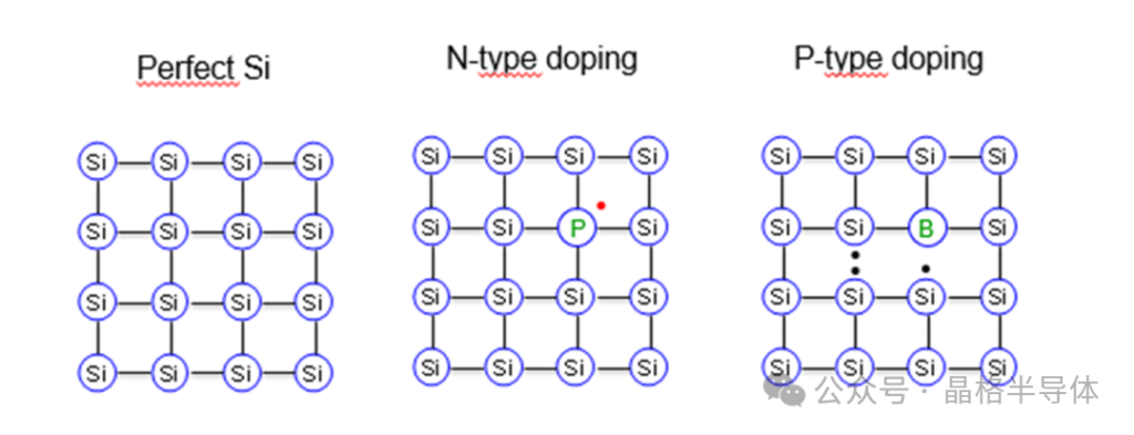
Answer: These are the two main branches of doping technology. The essential difference lies in the type of impurity introduced, which determines the type of charge carriers that conduct electricity.
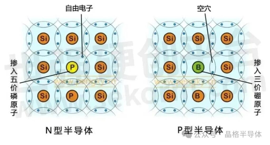
N‑type Doping – Supplies Electrons
- Elements: Group V elements – Phosphorus (P), Arsenic (As), Antimony (Sb)
- Atomic structure: These atoms have 5 valence electrons, one more than silicon (4)
- Conduction mechanism: The extra valence electron is easily freed to become a free electron; silicon conducts mainly via electrons (electrons are majority carriers)
- Typical applications: NMOS transistors, emitter regions of NPN bipolar transistors
P‑type Doping – Supplies Holes
- Elements: Group III elements – Boron (B), Gallium (Ga), Indium (In)
- Atomic structure: These atoms have only 3 valence electrons, one fewer than silicon
- Conduction mechanism: The missing electron creates a hole in the lattice; holes can move like positive charges and conduct electricity
- Typical applications: PMOS transistors, emitter regions of PNP bipolar transistors
Key mnemonic: N‑type = Negative (electron conduction) → dopants are to the right of silicon in the periodic table (Group V); P‑type = Positive (hole conduction) → dopants are to the left of silicon (Group III).
❓ What Are the Pros and Cons of the Four Doping Processes, and How to Choose?
Answer: Different doping processes suit different applications. The key trade‑offs are cost, precision, and damage.
| Doping Process | Principle | Key Advantages | Key Disadvantages | Typical Applications |
|---|---|---|---|---|
| Thermal Diffusion | Impurity atoms diffuse from high‑ to low‑concentration regions at high temperature (>900°C) | Simple equipment, low cost, batch processing | Concentration and depth cannot be independently controlled; high‑temperature defects | Deep junctions, power devices |
| Ion Implantation | Ionize impurity atoms → accelerate in electric field → directly “bombard” and implant into the silicon surface layer | Independent and precise control of concentration and depth; low temperature (<400°C) avoids thermal defects | Expensive equipment (millions of USD per unit); lattice damage requires annealing | Mainstream for modern ICs (source/drain doping, threshold adjustment) |
| In‑situ Doping | Mix dopant‑containing gases during epitaxial growth; the newly grown silicon layer is already doped | Precise control of doped layer thickness and concentration; abrupt interfaces | High process control requirements | Epitaxial base layers, heterojunction bipolar transistors |
| Neutron Transmutation Doping | Irradiate silicon with thermal neutrons; <sup>30</sup>Si → <sup>31</sup>P, uniform N‑type doping | Excellent uniformity (resistivity variation <5%) | Requires nuclear reactor; N‑type only; radioactive waste handling | High‑voltage high‑power devices (e.g., thyristors) |
Process selection guideline: High precision, small feature size → Ion Implantation; simple structures, cost‑sensitive → Thermal Diffusion; ultra‑thick layers, specific structures → In‑situ Doping; extreme uniformity requirements → Neutron Transmutation Doping.
❓ How Does Doping Concentration Affect Silicon Performance?
Answer: The inverse relationship between doping concentration and resistivity is central to doping control.
- Core relationship: Higher doping concentration → more carriers (electrons or holes) → lower resistivity → higher conductivity
- Control point: Precisely controlling the amount of dopant and its distribution in the lattice is key to achieving the target resistivity
- Typical ranges (for single‑crystal silicon):
| Doping Concentration Range (atoms/cm³) | Resistivity Range (Ω·cm) | Typical Applications |
|---|---|---|
| 10¹⁴ – 10¹⁵ | 10 – 100 | High‑resistivity epitaxial layers, detector substrates |
| 10¹⁵ – 10¹⁶ | 1 – 10 | General discrete devices, MEMS |
| 10¹⁶ – 10¹⁸ | 0.01 – 1 | IC substrates, power devices |
| > 10¹⁹ | < 0.001 | Heavily doped electrodes (ohmic contact layers) |
Key point: A small change in doping concentration (one order of magnitude) causes a similarly large change in resistivity (also about one order of magnitude) – which is precisely why doping technology demands extreme precision.
❓ Besides Modifying Conductivity, What Other Special Applications Does Doping Have?
Answer: Doping is not only used to change conductivity type and resistivity; it can also introduce specific “impurity levels” to achieve special functions.
Special Doping – Lifetime Control
Introducing heavy metal impurities such as gold (Au) or platinum (Pt) creates deep levels in the silicon bandgap, forming efficient recombination centres that can substantially shorten minority carrier lifetime.
- Typical applications: High‑speed switching devices where fast recombination of minority carriers reduces storage time and increases switching speed
- Control key: The doping concentration determines recombination efficiency and must precisely balance the trade‑off between “switching speed” and “on‑state voltage drop”
Other Special Dopants
- Germanium (Ge) : For SiGe heterojunctions (SiGe HBT) to enhance high‑frequency performance
- Carbon (C) : For strain engineering to improve carrier mobility (strained‑silicon technology)
- Oxygen (O) : For mechanical strength enhancement via intrinsic gettering
❓ How Do Doping Requirements Differ Across Various Application Fields?
| Application Area | Main Doping Requirements | Key Parameters | Core Concerns |
|---|---|---|---|
| Logic Chips (CPU/GPU) | Ultra‑shallow junctions, high precision | Implantation energy, dose | Short‑channel effect control, threshold voltage uniformity |
| Memory Chips (DRAM/NAND) | Large‑area uniformity | Doping uniformity, annealing conditions | Leakage control, data retention characteristics |
| Power Devices (IGBT/MOSFET) | Deep junctions, high concentration | Diffusion depth, surface concentration | Breakdown voltage vs. on‑resistance trade‑off |
| Detectors/Sensors | Ultra‑low concentration, high‑purity substrates | Intrinsic gettering, compensation control | Signal‑to‑noise ratio, dark current suppression |
| MEMS | Multiple doping types integrated | Selective doping, thermal budget control | Mechanical stress vs. electrical performance coordination |
Article source: Jingge Semiconductor — Supplies ultra‑large single crystal silicon, multi crystalline silicon columnar‑grained materials, and offers OEM custom fabrication of Si parts, including etch rings, shower heads, exhaust rings, focus rings, and shield rings.