During the Czochralski (CZ) growth of monocrystalline silicon ingots, the thermal shock generated when the seed crystal contacts the melt inevitably introduces a high density of dislocations at the seed end. If not intervened, these dislocations will proliferate exponentially according to the Alexander‑Haasen model, rendering the entire monocrystalline silicon ingot unusable for device fabrication. The Dash necking process, invented by W.C. Dash in 1958–1959, grows a thin neck of 2–4 mm in diameter and 100–150 mm in length at the initial stage by employing a high pulling rate. This neck provides a short path for dislocation slip and climb to the free surface, where they annihilate, thereby physically truncating the defect inheritance from the seed crystal. This paper systematically reviews the origin of thermal‑shock dislocations, the exclusion mechanism of the Dash necking, key process parameters, engineering constraints, and the challenges posed by large‑diameter silicon ingot production, as well as alternative approaches such as heavily doped seed crystals.
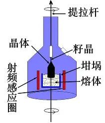
1. Origin of Dislocations: Thermal Shock at the Seed–Melt Contact
In the CZ process, a monocrystalline silicon seed crystal (typically 〈100〉 or 〈111〉, ~10×10 mm² cross‑section) is lowered to touch the molten silicon (~1420°C). The huge temperature gradient between the seed top and its bottom induces intense thermal stress. When this stress exceeds the critical resolved shear stress (CRSS) of silicon at high temperature, the {111}〈110〉 slip systems are activated, generating a large number of slip dislocations. Even if the seed crystal is initially dislocation‑free, the dipping process almost inevitably introduces dislocations. These dislocations, if left untreated, will propagate into the growing monocrystalline silicon ingot and multiply exponentially under growth stresses.
2. Dislocation Elimination Mechanism of the Dash Necking
2.1 Basic Operation
After seeding, the pulling rate is rapidly increased to 2–6 mm/min, reducing the grown diameter to 2–4 mm. This thin neck is maintained for 100–150 mm in length, after which the rate is reduced and the shoulder is enlarged to the target diameter (200–450 mm).
2.2 Dislocation Slip to the Surface
In silicon, dislocations glide on {111} planes along 〈110〉 directions. In a normal‑diameter crystal, the distance from the slip plane to the lateral surface is long, so dislocations tend to propagate along the growth axis. However, when the neck diameter is reduced to only 2–4 mm, the glide path to the surface is drastically shortened. Dislocations can reach the free surface within a short distance; once at the surface, the Burgers vector is terminated, and the dislocation annihilates. This mechanism is the core of the Dash necking process: it does not prevent dislocation generation but provides an ultra‑short escape route to the surface, ensuring the final monocrystalline silicon ingot is dislocation‑free.
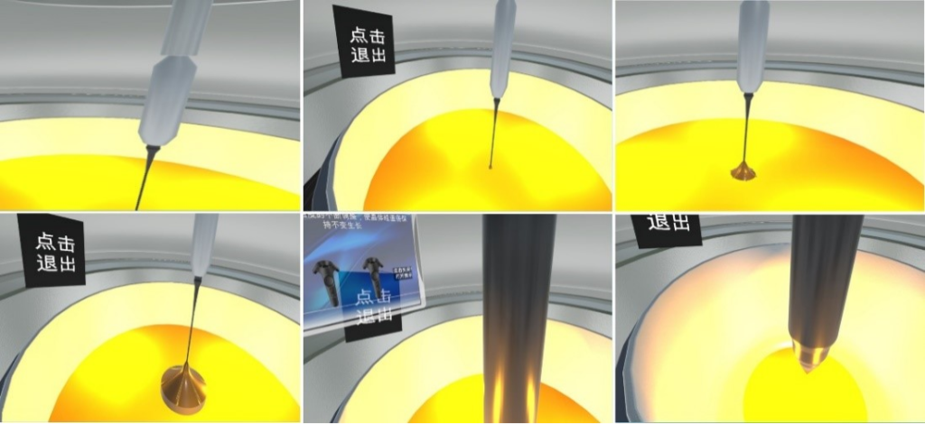
2.3 Climb and Half‑Loop Expansion – Synchrotron X‑ray Topography Evidence
Kawado et al., using SPring‑8 synchrotron white X‑ray topography, observed that in the transition region from the dislocated zone to the dislocation‑free zone, dislocation half‑loops are generated, expand on {111} planes, and eventually terminate inside or reach the side surface. This confirms that both slip‑to‑surface annihilation and vacancy‑assisted climb contribute to the elimination process.
2.4 Kinetic Criterion: Pulling Rate Faster than Dislocation Velocity
A simple but effective description is that the pulling speed exceeds the dislocation motion speed. In the thin neck, the high cooling rate reduces thermal stress, and the fast interface movement leaves dislocations behind, either captured by the surface or unable to keep up with the advancing solidification front.
3. Key Parameters and Engineering Constraints
3.1 Critical Diameter: 2–4 mm
The maximum diameter for effective dislocation elimination is about 4 mm. Beyond this, the slip path becomes too long, and some dislocations survive into the shoulder and the main monocrystalline silicon ingot.
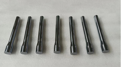
3.2 Neck Length: 100–150 mm
The exclusion process requires a sufficient buffer length. Topography data show that dislocation density gradually decreases over several tens of millimeters before reaching zero.
3.3 Mechanical Bottleneck – Load‑Bearing Capacity
A 3–4 mm silicon neck must support the entire weight of the growing monocrystalline silicon ingot, which for 300 mm diameter exceeds 300 kg. Fracture occurs at the neck‑shoulder junction. For 450 mm ingots, the required neck diameter for mechanical strength (>8 mm) conflicts with the 4‑mm limit for dislocation elimination. This is the fundamental paradox of large‑diameter CZ growth.
4. Advanced Challenges and Alternative Routes
4.1 Scaling to 300 mm and 450 mm
Traditional Dash necking is approaching its physical limit. Optimized shoulder shapes can reduce stress but cannot fully resolve the conflict.
4.2 Neckless Growth with Heavily Doped Seeds
It has been found that boron‑doped seeds (B ~1×10¹⁸ cm⁻³) can yield dislocation‑free monocrystalline silicon ingots without necking, due to impurity locking of dislocations. Germanium‑ or indium‑doped seeds also show similar effects. This offers a potential path for ultra‑large ingots (>500 kg), though issues such as dislocation loops generated during thermal cycling and seed reuse remain.
4.3 Paradigm Shift toward Defect Engineering
While Dash necking ensures the fundamental dislocation‑free status of the monocrystalline silicon ingot, modern growth also focuses on controlling point defects (vacancies/interstitials) via the V/G criterion. Defect engineering allows intentional formation of bulk microdefects for gettering purposes, shifting the emphasis from “total elimination” to “controlled design.”
5. Conclusion
The Dash necking process is a brilliant engineering invention that physically intercepts the dislocation inheritance from the seed crystal. Its effectiveness relies on three conditions: (1) a thin neck that shortens the glide path to the surface; (2) half‑loop expansion and surface pinning; and (3) a pulling rate faster than dislocation motion. However, the mechanical–dislocation conflict becomes critical for 450‑mm monocrystalline silicon ingots. Neckless techniques using heavily doped seeds and advanced defect engineering represent the future directions for high‑quality, large‑diameter silicon crystal production.
Article source: Jingge Semiconductor — Providing ultra-large-size monocrystalline silicon materials, polysilicon columnar-grain materials, and custom processing of Si parts, silicon components, silicon targets, silicon electrodes, silicon rings, silicon barrels, silicon wafers, etc.