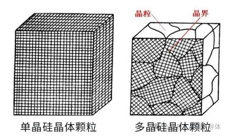
Grain boundaries in Multi Crystalline Silicon fall into three major categories: high-angle grain boundaries, low-angle grain boundaries, and twin boundaries. Their essential difference lies in — high-angle grain boundaries are “collision lines” formed by the encounter of grains with different orientations, low-angle grain boundaries are “queue walls” of neatly aligned dislocations, and twin boundaries are “mirror surfaces” created by atomic stacking faults.
Quick Comparison of the Three Grain Boundary Types
| Grain Boundary Type | Misorientation | Essence | Primary Formation Cause |
|---|---|---|---|
| High-Angle Grain Boundary | > 15° | Atomically disordered transition layer | Random nucleation + collision |
| Low-Angle Grain Boundary | < 10°–15° | Regular array of dislocations | Thermal stress → dislocation rearrangement |
| Twin Boundary | 60° (special) | Mirror-symmetric coherent interface | Atomic layer stacking fault |
❓ What is a High-Angle Grain Boundary and How Does It Form?
Answer:
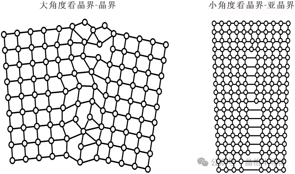
A high-angle grain boundary is the interface between grains with a misorientation exceeding 15°. The atomic arrangements on the two sides differ greatly, making a smooth transition impossible, thus forming a disordered transition layer several nanometers thick (locally nearly amorphous).
Three Formation Mechanisms
Mechanism 1: Random Nucleation and Growth Collision (Primary Cause)
Silicon melt crystallizes simultaneously at countless points on the bottom and side walls of the crucible, with each nucleus having a completely random atomic orientation. As these tiny grains grow, they inevitably “collide” at some location. When two grains with vastly different orientations meet, the atoms cannot align one-to-one, forcing the formation of a disordered transition layer — this is the precursor of a high-angle grain boundary.
Mechanism 2: Boundaries of Survivors After Competitive Growth
During directional solidification, only grains whose growth direction (<100>) is roughly parallel to the heat flow direction can grow upward, eliminating unfavorably oriented “neighbors.” The interfaces between the ultimately surviving columnar grains constitute the backbone network of high-angle grain boundaries. This is also why, after the ingot is cut, the grain boundaries appear as a longitudinally penetrating network pattern.
Mechanism 3: Dendrite Encounter
When constitutional supercooling occurs, the crystal grows in a dendritic manner. Different dendrite arms or dendrite networks from different nuclei intersect and collide within the melt, also forming high-angle grain boundaries.
Core Characteristics: High interfacial energy, strong electrical activity, and act as strong recombination centers for minority carriers.
❓ What is a Low-Angle Grain Boundary and What is Its Relationship with Dislocations?
Answer:
A low-angle grain boundary has a misorientation typically less than 10°–15° on either side. It is essentially not a “plane,” but a “queue wall” composed of a series of regularly arranged dislocations.
Formation Mechanisms
Mechanism 1: Thermal Stress-Driven Dislocation Slip and Climb (Primary Cause)
When a silicon ingot cools from above 1400°C, a huge temperature gradient exists internally, generating intense thermal stress. When the stress exceeds the critical value, the crystal releases stress through the generation and movement of dislocations. Dislocation lines slip within the crystal and tend to entangle and pile up with one another.
Mechanism 2: Polygonization of Dislocations
At high temperatures (approximately above 1000°C), dislocations that were originally randomly distributed undergo spontaneous rearrangement to reduce the total elastic energy of the system. They align themselves regularly like soldiers forming ranks, creating a “wall.” The crystal lattices on the two sides of this “dislocation wall” thus develop a small misorientation.
Depending on the arrangement of dislocations, low-angle grain boundaries are further divided into two types:
- Tilt Boundary: Composed of a vertical array of edge dislocations of the same sign, like a stack of blades inserted into the crystal, causing the lattices on either side to tilt by a certain angle around an axis.
- Twist Boundary: Composed of two sets of screw dislocations intersecting in a grid pattern, causing the lattices on either side to twist around an axis perpendicular to the interface.
Core Characteristics: Relatively low interfacial energy, and much weaker electrical activity than high-angle grain boundaries. However, the dislocations themselves (especially when “decorated” by metallic impurities such as iron or copper) can also become recombination centers.
Article source: Jingge Semiconductor — Supplies ultra‑large single crystal silicon, multi crystalline silicon columnar‑grained materials, and offers OEM custom fabrication of Si parts, including etch rings, shower heads, exhaust rings, focus rings, and shield rings.