1. Introduction: The Challenge of Casting Polysilicon
The conventional manufacturing process for polysilicon involves placing raw silicon feedstock into a crucible, heating it to complete melting, and then adjusting the position of the crucible or heater to establish a vertical temperature gradient within the melt—from bottom to top—to initiate directional solidification. Upon completion of solidification, a polysilicon ingot is obtained.
However, this casting process introduces significant challenges. During directional solidification, thermal stresses generate a substantial number of dislocations. Moreover, the crucible itself introduces contamination—impurities leach into the silicon feedstock—and the presence of grain boundaries profoundly affects crystal growth. The inherent instability of crystal growth during directional solidification often leads to internal defects and even impurity aggregation. Therefore, controlling crystal growth and impurity distribution is of critical importance for improving the quality of cast polysilicon ingots.
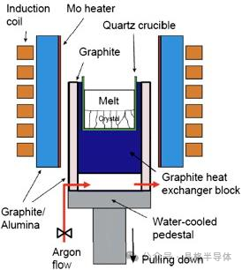
2. Strategies for Quality Improvement: Simulating Monocrystalline Silicon
Polysilicon produced by the directional solidification casting method contains high densities of dislocations and impurity defects, making its quality far inferior to that of dislocation-free monocrystalline silicon grown by the Czochralski (CZ) process.
To emulate monocrystalline silicon and achieve comparable performance—while simultaneously improving the quality of cast polysilicon ingots—extensive research has focused on growing large grains with numerous electrically inactive grain boundaries. Two representative approaches have emerged as typical methods: cast-mono silicon technology and dendritic casting technology.
2.1 Cast-Mono Silicon Technology (Seed-Assisted Growth)
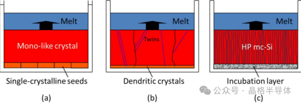
As illustrated in Figure (a), this approach places multiple seed crystals (monocrystalline silicon pieces) at the bottom of the crucible. Through epitaxial growth from these seeds, monocrystalline silicon is produced.
2.2 Dendritic Casting Technology
As shown in Figure (b), this method leverages the faceted growth properties of silicon. Under high cooling rates, it induces the growth of large-columnar-grain crystals—hence the name dendritic casting.
Both technologies aim to improve the quality of directionally solidified silicon ingots by growing large-grain-size crystals and thereby reducing the number of grain boundaries.
2.3 Limitations of These Approaches
Despite attracting considerable research attention after its introduction, cast-mono silicon technology has faced developmental constraints. Issues such as polysilicon incursion and the introduction of extensive dislocation defects at the seams where seed crystals are joined have limited its progress, and its period of active development was relatively short.
For the dendritic casting method, two major challenges persist. First, the degree of undercooling is difficult to control precisely. Second, even when large columnar grains are successfully induced, substantial dislocation clusters inevitably arise due to thermal stresses, significantly degrading the quality of the resulting polysilicon.
3. High-Performance Casting Polysilicon Technology: A Breakthrough Approach
To ensure high-quality silicon ingots while simultaneously reducing dislocation proliferation and propagation, Jingge Semiconductor has developed high-performance casting polysilicon (HP cast polysilicon) technology.
As depicted in Figure (c), this method employs small silicon particles or silicon chunks as a seed nucleation layer to assist crystal growth, resulting in a vertically oriented columnar grain structure.
3.1 How It Works: From Fine Grains to High Performance
This HP columnar-grain polysilicon technology has had a significant impact on semiconductor components. Unlike traditional approaches that focus on growing large grains with electrically inactive twin boundaries, HP polysilicon initiates crystal growth from uniform fine grains containing numerous random grain boundaries.
Growing grains from this fine-grain structure at the base provides several critical benefits:
- Significant mitigation of thermal stress
- Suppression of dislocation cluster formation and propagation
3.2 Nucleation Control Methods
Beyond using silicon particles as seed crystals to induce large-grain growth, the nucleation process can also be controlled by applying a nucleation agent coating—offering an additional pathway to achieve high-performance cast polysilicon.
4. Cast-Mono vs. HP Cast Polysilicon: A Comparative Analysis
Although both cast-mono silicon technology and high-performance casting polysilicon technology are seed-induced ingot growth techniques, they exhibit fundamental differences:
| Aspect | Cast-Mono Silicon | HP Cast Polysilicon |
|---|---|---|
| Seed Material | Monocrystalline silicon wafers/pieces | Small polysilicon chunks or particles |
| Production Cost | Higher (requires single-crystal seeds) | Lower (uses inexpensive polysilicon feedstock) |
| Defect Behavior | Seam-induced dislocations proliferate rapidly due to absence of grain boundaries | Grain boundaries hinder dislocation propagation and reduce dislocation density |
| Grain Boundary Characteristics | Not applicable | Relatively straight grain boundaries with columnar grain morphology |
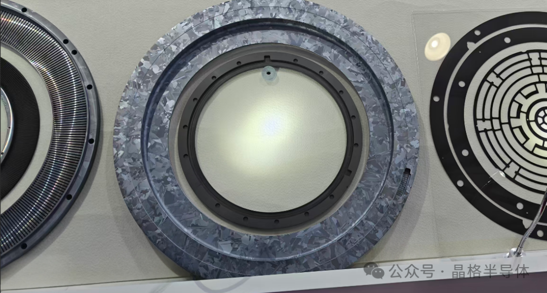
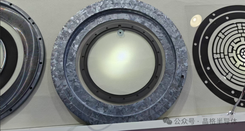
The presence of grain boundaries in HP cast polysilicon—which are relatively straight and grow in a columnar-grain pattern—effectively blocks dislocation propagation and reduces dislocation density. Silicon ingots produced via this technology, when processed into silicon components, exhibit superior performance characteristics.
Article source: Jingge Semiconductor — Providing ultra-large-size monocrystalline silicon materials, polysilicon columnar-grain materials, and custom processing of Si parts, silicon components, silicon targets, silicon electrodes, silicon rings, silicon barrels, silicon wafers, etc.